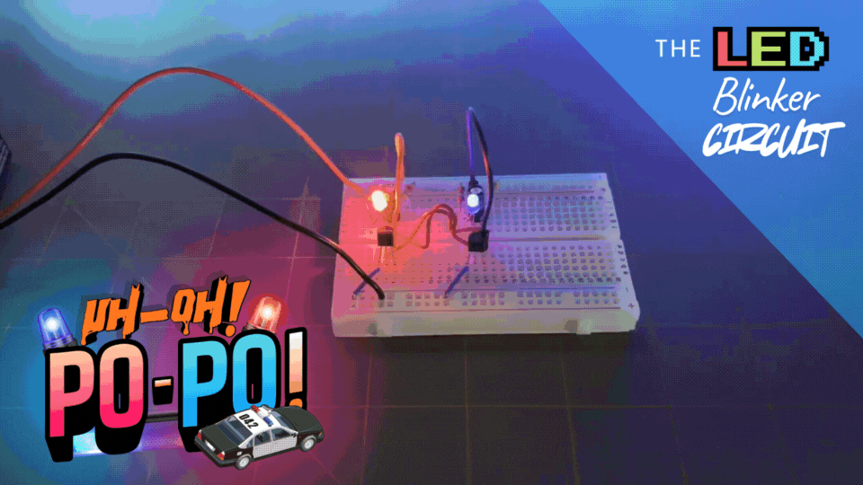
Gaining a Deeper Understanding of the LED Blinker Circuit (An Extended Topic for the LED Blinker Circuit)
Introduction
The following content is intended to be a companion to the LED blinker circuit we created from our article titled, “How Components Work Together in Real Circuits.”
The sole purpose of this discussion is to work as an extended topic for that article to help you understand your circuit better, to help clarify what’s actually happening within it, and to gain a deeper understanding of its inner workings.
The following is meant to be thorough, and codified in a way to be understandable to any reader, no matter their background, thought process, or way of learning — at least we hope that it is. There have been several different attempts to express the content for this discussion here in hopes to be accessible for all.
We hope that you find the following to be useful.

🧐 How Did We Get Here?
Where we started:
We were learning about components in the Circuit Component Super Series, and in Part 3 of that series we learned that by putting together some of these components in a particular way, we could build a blinking LED circuit. This LED Blinker Circuit led us toward a separate, but companion topic of discussion to the Circuit Component Super Series, which in itself turned into its own subseries called the Astable Multivibrator Subseries. This will be the third and final installment of this subseries.
What we learned next:
We then learned that the LED blinker circuit we made in How Components Work Together in Real Circuits was a special kind of circuit called an astable multivibrator — we learned about some of the history behind the astable multivibrator and how our blinker circuit worked, explained in several different ways.

What we just learned:
In the previous companion article to this one, we went over some common questions asked about our LED blinker circuit. We went over topics like: electron flow through the circuit, base current and resistance at the transistors of the circuit, and other pertinent information about the LED blinker circuit.
What we’re learning here:
For this final installment of this Astable Multivibrator Subseries, we will be diving deep into how the blinker circuit works, how calculations are made for it, and how we can use those calculations to manipulate our circuit into performing the way we want.
Once you’re done with this third and final installment of this Astable Multivibrator Subseries, you can proceed on to Part 4, of our Circuit Component Super Series, if you haven’t done so already.

🗺️ The LED Blinker Circuit Schematic
I’ve provided the LED Blinker Circuit schematic here, so that we may refer to it throughout our discussion. Click on the image so that you may open it in another tab to download it, if you need to.

🤿 A Deep Dive Into Understanding the LED Blinker Circuit
If you read our article titled, “What Exactly is an Astable Multivibrator?,” you might recall that the term “vibrator” is used to describe circuits that:
- Flip
- Toggle
- Switch abruptly
- And “snap” between voltage levels
That a multivibrator is simply a circuit with multiple switching states — in our case, our LED blinker circuit switches a couple LEDs on and off continually. This means that if we could graphically see what was happening within our circuit, we’d “see” that voltage is applied to an LED, then not, then applied again, then not — over and over again.
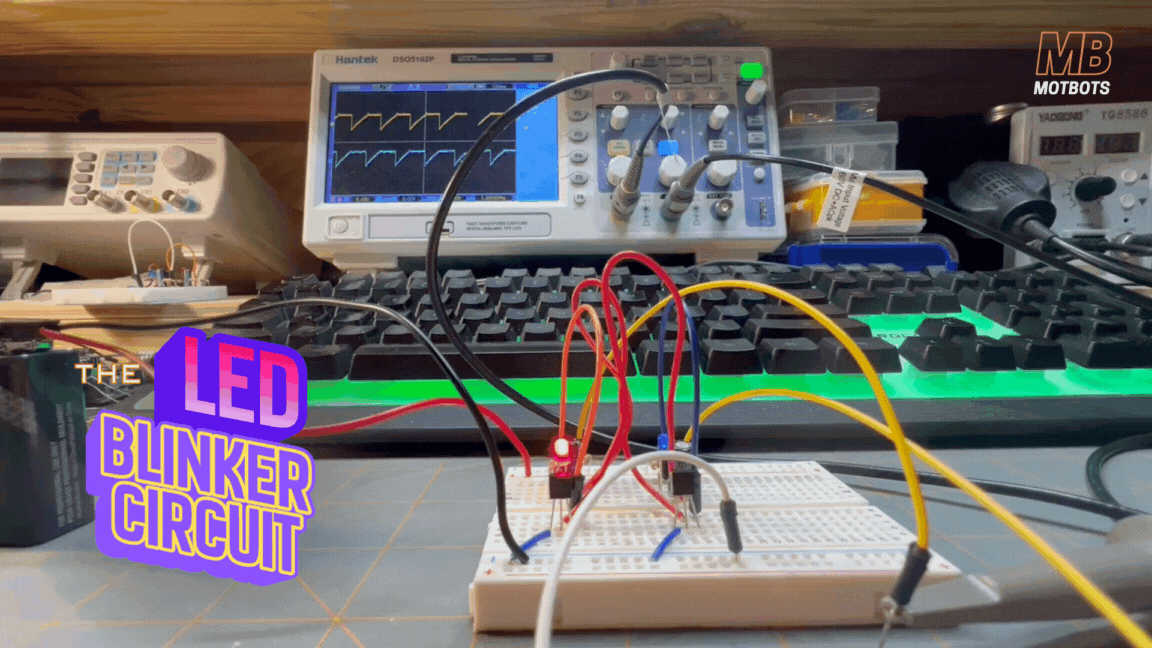
Essentially, our LED blinker circuit is a square-wave generator. Looking at the image below, you can see where I’ve connected a couple of oscilloscope probes across the red LED in the blinker circuit.
- When the red LED is ON, we see an immediate sign of voltage shown across it on the graph, on the display screen of the oscilloscope.
- When the red LED is OFF, we see no sign of voltage (or 0V) shown across it on the graph, on the display screen of the oscilloscope.
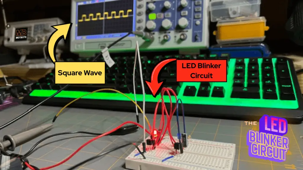
This continual ON, OFF, ON, OFF on the graph shows a square-wave of voltage across the LED when on and 0V across the LED when off. This square-wave simply tells us that there’s either a certain amount of voltage across the LED at a given instant of time, or there isn’t — it’s that simple.
Let’s take a closer look at those waveforms, next.
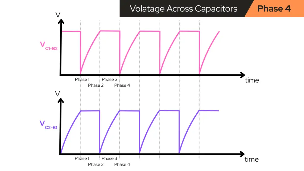
👣 Walking Through the Waveforms
Let’s walk through the waveforms of our LED blinker circuit. We will walk through the exact voltage waveforms on:
- The collector of Q1
- The collector of Q2
- Capacitor C1
- And capacitor C2
We’ll also use a frame-by-frame time-graph graphic of one full blink cycle of the LED blinker circuit, describing the waveforms in simple terms (high/low, rising/falling) rather than drowning you in calculus.
Let’s first assume the usual astable setup we built:
- Transistor (Q1) is the red LED side
- Transistor (Q2) is the blue LED side
- Capacitor (C1) goes from Q1 collector to Q2 base
- Capacitor (C2) goes from Q2 collector to Q1 base
- Each collector has a resistor up to +9V and an LED path to ground
- Both emitters are at ground
We’ll track the following voltages:
- VC1: The voltage at Q1’s collector (red LED node)
- VC2: The voltage at Q2’s collector (blue LED node)
- VB1: Q1’s base voltage
- VB2: Q2’s base voltage
- VC1-B2: The voltage across C1 (Q1 collector to Q2 base)
- VC2-B1: The voltage across C2 (Q2 collector to Q1 base)
We’ll use the following simple labels to describe the waveforms and what’s going on within the circuit itself:
- “HIGH”: Approximately or near +9V
- “LOW”: Approximately or near 0V
- “Rising”: Slowly going up
- “Falling”: Slowly going down
- “Spike”/”Kick”: Fast jump up or down
So now that we have some of the preliminaries out of the way, let’s go take a walk!
Phase 0 – Just Before the Blink (at Power-Up)
As we start a walk through of the waveform of the blinker circuit, let’s first observe what’s going on right as we first connect the 9V battery to it:
- Both capacitors C1 and C2 are uncharged (0V across them).
- Both transistors want to turn on (they both get some base influence through the resistors and capacitors).
- Because of tiny imperfections, one transistor will win the race by a hair.
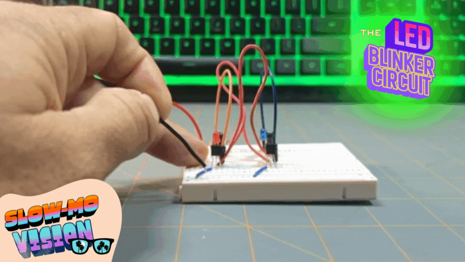
We can see this happening using our “slow-mo vision,” and see that when power is applied to the circuit, initially the two transistors act as if they both want to turn on, but the red LED ultimately wins and is the first to turn on.
Now we start our frame-by-frame graphic at the moment Q1 has just turned on fully.
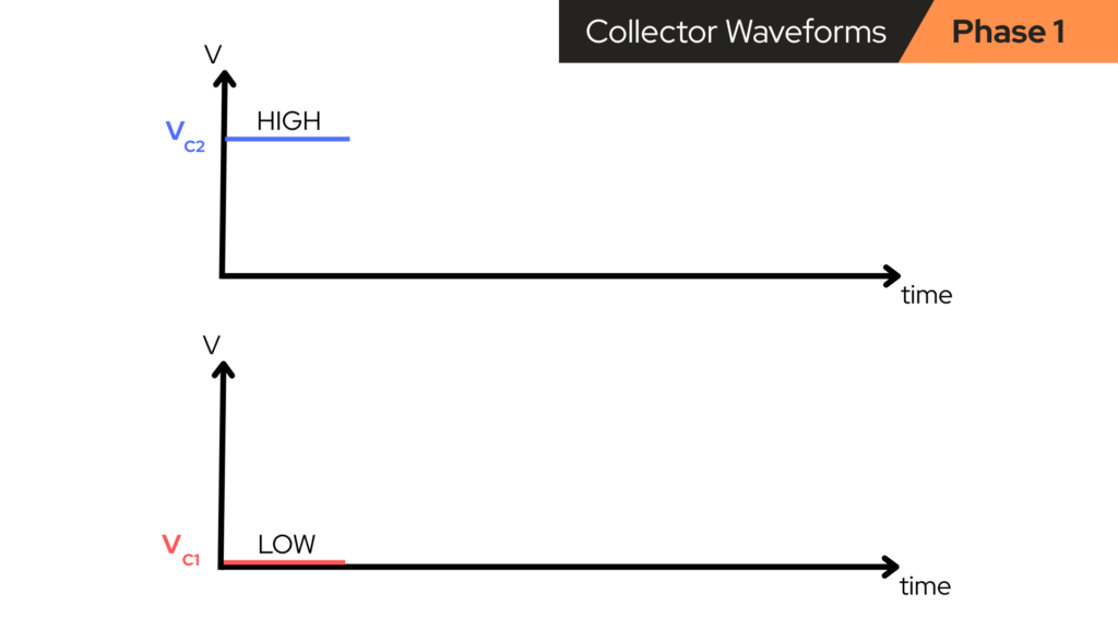
Phase 1 – Red ON, Blue OFF (Q1 ON, Q2 OFF)
After power is applied to the circuit, Q1 wins and the red LED turns on. What the main nodes are doing now are as follows:
- Transistor Q1 is ON and the voltage at Q1’s collector (VC1) is LOW
- Q1 is conducting from collector to emitter (down to ground).
- So, the voltage at the collector of Q1 is: VC1 ≈ 0V (LOW).
- There’s current flowing through the red LED, so the red LED is ON.
- Transistor Q2 is OFF and the voltage at Q2’s collector (VC2) is HIGH
- Q2 is not conducting, so its collector is pulled up through its resistor to +9V.
- So, the voltage at the collector of Q2 is: VC2 ≈ 9V (HIGH).
- The blue LED has no path to ground for electrical current, so the blue LED is OFF.
So at this stage the collector waveforms are:
- VC1: LOW (~0V)
- VC2: HIGH (~9V)
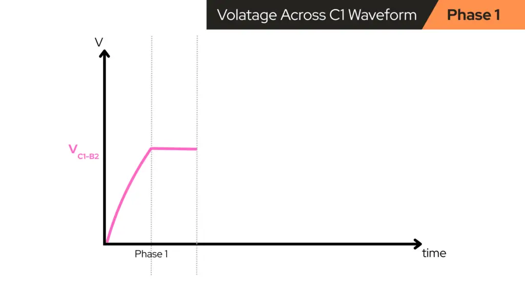
What happens to C1 (between Q1 collector and Q2 base)
Capacitor C1, connects transistor Q1’s collector (VC1) to transistor Q2’s base (VB2). When Q1 snapped ON a moment ago:
- VC1 dropped quickly from HIGH (~9V) to LOW (~0V).
- Capacitors resist sudden changes in voltage across themselves, so:
- When the collector side of C1 jumps downward,
- C1 drags Q2’s base downward with it for a short moment.
That creates a sharp negative “kick” on Q2’s base:
- VB2 gets yanked downwards (can even go slightly negative).
- This strongly turns Q2 OFF, ensuring it loses the startup race.
Right after that kick:
- Q2’s base is very low, therefore Q2 is OFF.
- C1 now has some voltage stored across it (because one side moved, the other followed temporarily, and then currents start to flow to “relax” it).
During Phase 1, C1 is now:
- Slowly charging/discharging through resistors toward a new balance.
- That means VB2 (Q2’s base) starts slowly rising from that negative level back toward its normal “turn-on” threshold (~0.6V or so).
So, roughly:
- VB2: starts low, then rises slowly over time.
- VC1–B2 (voltage across C1): starts at some value and gradually changes as C1 charges. The shape of its curve is a smooth exponential curve, not a sharp jump.
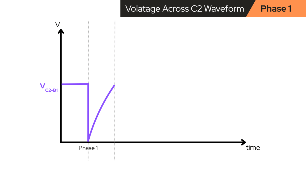
What happens to C2 (between Q2 collector and Q1 base)
Capacitor C2, connects transistor Q2’s collector (VC2 = HIGH) to transistor Q1’s base (VB1 ≈ 0.6V, because Q1 is ON).
- With Q2 OFF (VC2 HIGH) and Q1 ON (VB1 ≈ 0.6V),
- There’s a fairly constant difference across C2.
Over this part of the cycle, C2 mostly just sits at a nearly steady voltage; it isn’t doing anything dramatic yet. It’s “getting ready” for the next flip.
So, in Phase 1:
- VB1 (Q1 base): stays around “on level” (~0.6–0.7V).
- VC2–B1 (voltage across C2): slowly drifts or holds near a fixed value; nothing explosive.
Phase 2 – The Flip to Blue ON (Q2 turns ON, Q1 turns OFF)
Eventually, during Phase 1, Q2’s base voltage (VB2) rises high enough (after that negative kick has “worn off”) that Q2 begins to turn ON. The moment Q2 turns ON:
- Q2’s collector drops from HIGH to LOW
- VC2 goes from ~9V down to near 0V, quickly.
- This is just like what happened on Q1’s collector earlier, but on the blue side now.
- That sudden drop at VC2 is connected through capacitor C2 to Q1’s base (VB1).
- C2 doesn’t like its voltage changing instantly, so it “kicks” Q1’s base downward.
- Q1’s base voltage VB1 suddenly drops, shutting Q1 OFF.
- As soon as Q1 turns OFF, VC1 rises (back up toward +9V) through its collector resistor.
- The red LED loses its path to ground, so the red LED turns OFF.
At this exact switch moment, the collector waveforms do the following, as seen in the image below:
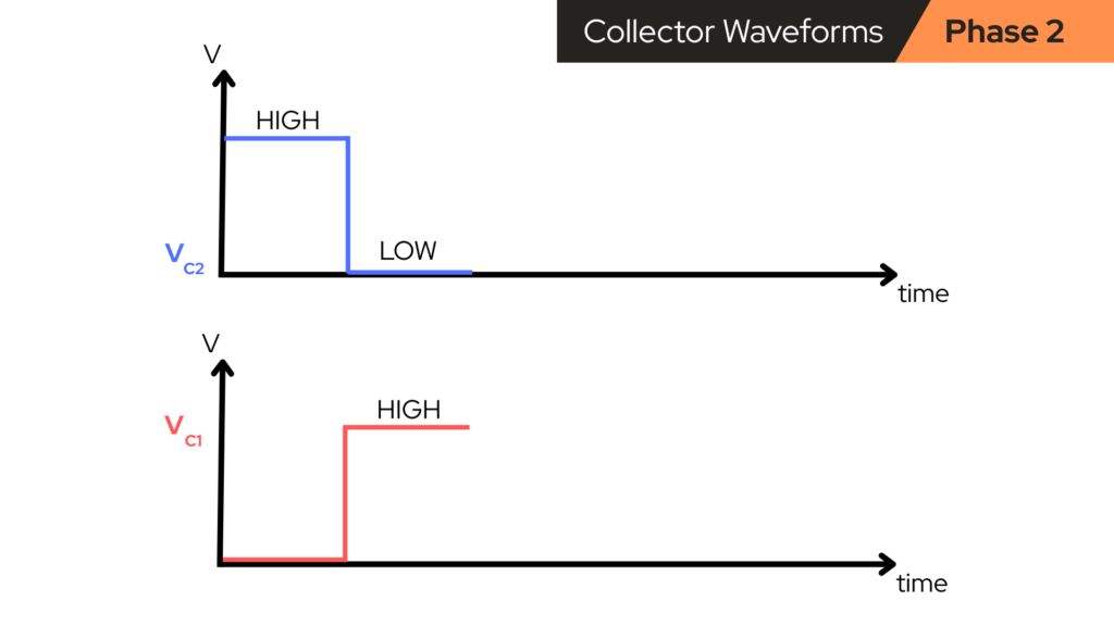
In simple words:
- VC1 jumps from LOW to HIGH.
- VC2 jumps from HIGH to LOW.
- The red LED goes OFF and the blue LED goes ON.
Now we’re in the opposite state:
- Q1 goes OFF, VC1 becomes HIGH, and the red LED turns OFF
- Q2 goes ON, VC2 becomes LOW, and the blue LED turns ON
Phase 3 – Blue ON, Red OFF (Q2 ON, Q1 OFF)
Now we repeat the same kind of behavior, just mirrored:
- Transistor Q2 is nowON. So, VC2becomesLOW and the blue LED goes ON.
- Transistor Q1 is now OFF. So, VC1 becomes HIGH and the red LED goes OFF.
C2 Behavior in This Phase
Remember that capacitor C2 connects the collector voltage of Q2 (VC2) and the base voltage of Q1 (VB1).
- When Q2 turned ON, VC2 dropped suddenly, and C2 dragged VB1 down, kicking Q1 OFF.
- Now, in this phase, C2 begins to relax and it slowly charges/discharges through the resistors, so VB1 slowly rises again toward the level where Q1 will turn back ON.
So during Phase 3, VB1 is slowly rising from a low level back toward ~0.6V. The voltage across capacitor C2 (VC2-B1) changes smoothly as C2 charges — looks like a gentle exponential curve.
C1 behavior now
C1 is now connected between VC1, which is HIGH (Q1 OFF), and VB2, which is approximately 0.6V (Q2 ON). So C1 just holds a nearly constant voltage for most of this phase, waiting for the next flip.
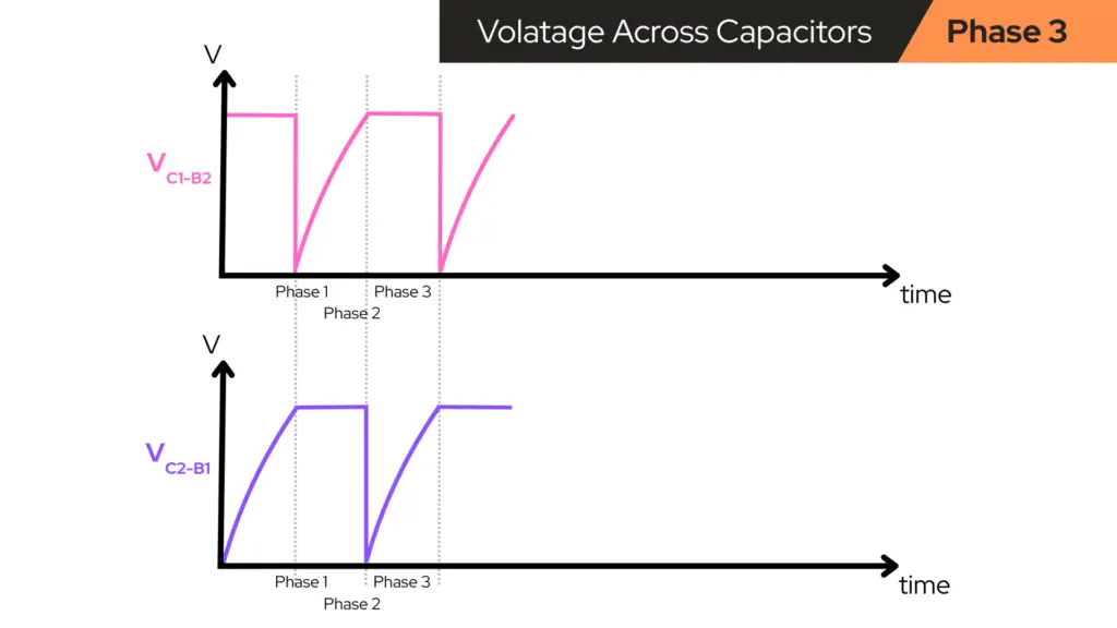
Phase 4 – Flip back to Red ON
Eventually, as C2’s “hold” wears off, VB1 gets high enough to turn Q1 back ON. When that happens:
- Q1 turns ON and VC1 drops from HIGH to LOW.
- C1 passes that sudden drop to Q2’s base (VB2) and Q2 gets kicked OFF.
- VC2 rises from LOW to HIGH.
- The red LED comes back ON and the blue LED turns OFF.
Now we’re back to the beginning: Phase 1 again (red ON, blue OFF), and the whole cycle repeats.
Why the Components Blink (The Secret Weapon: Capacitors!)
The magic of the circuit comes from two facts:
1. Transistors react instantly
When their base voltage crosses a certain level, they switch fast.
2. Capacitors react slowly — except when something changes suddenly
If one side of a capacitor moves slowly, then the capacitor allows the voltage to “settle.” But if one side suddenly jumps or drops, then the capacitor throws that change onto the other side.
With our LED blinker circuit:
- The slow part (charging) controls the timing.
- The fast part (kicks) flips who’s “in charge” of the blinking.
This combination is why the circuit oscillates:
- One transistor turning on forces the other to turn off,
- and then the capacitors slowly “count” until it’s time to flip roles.
How Your Circuit Achieves Oscillation
The LED blinker circuit we created back in Part 3 of our Circuit Component Super Series uses:
- two NPN transistors (PN2222),
- two timing resistors (R3 and R4),
- two timing capacitors (C1 and C2),
- and two LEDs and their current limiting resistors.
The oscillation comes from a feedback loop created by the resistor-capacitor (RC) network that cross-connects the collector of each transistor to the base of the other. This RC network determines when each transistor turns ON.
🤔 Why it ACTUALLY Oscillates
1. One transistor “wins” at power-on
Real components always differ slightly, so one LED turns on first. Let’s say Q1 turns on first:
- Q1’s LED lights
- Q1 pulls its collector low
- The falling voltage at Q1’s collector drags C1 negative
- That negative voltage hits Q2’s base, forcing Q2 OFF
2. Capacitor C1 slowly charges through R3
C1 begins climbing back up toward 0V. This slow rise is the timing function. As C1 creeps upward through R3:
- Q2’s base voltage rises with it
- Once it reaches ~0.6–0.7V, Q2 suddenly switches ON.
3. Q2 suddenly switches ON
The moment Q2 turns on:
- Its LED lights
- Q2’s collector voltage falls sharply
- C2 is yanked negative
- Negative voltage slams into Q1’s base
- Q1 switches OFF
This is the flip.
4. Then everything happens in reverse
C2 begins charging up through R4. When it rises far enough, Q1 snaps ON again and the cycle repeats forever.

Why the Capacitors Are Polarized the Way They Are
Looking at capacitor C1 in the schematic diagram of the LED blinker circuit shared above, we see that:
- The positive (+) side of C1 faces transistor Q1’s collector (usually HIGH when Q1 is OFF).
- The negative (-) side of C1 faces transistor Q2’s base (usually LOW when Q2 is OFF or during switching).
The same goes for capacitor C2, where:
- The positive (+) side of C2 faces transistor Q2’s collector.
- The negative (-) side of C2 faces transistor Q1’s base.
This means that capacitors always charge “right way around.” Their discharging into the other base provides the correct timing pulse. Reverse them and the circuit stops blinking or damages the caps.
The LED Blinker Circuit Uses Four Resistors
In the LED blinker circuit we made (a two-transistor astable multivibrator), we had a total of four resistors that were used within that circuit. Looking at the schematic diagram of the LED blinker circuit shared above, we observe that:
- R1 & R2 arethe LED current-limiting resistors. These are in series with each LED to prevent it from burning out.
- R3 & R4 are thebase/collector network resistors. These connect from the collector of Q1 to the base of Q2, and from the collector of Q2 to the base of Q1. These two resistors set:
- The blink timing
- How strongly one transistor influences the other
- The charging/discharging rate of the capacitors
- The bias level going into each base
In our circuit, there are no dedicated collector pull-up resistors (as sometimes shown in textbook astables). Instead, the LEDs and their resistors act as part of the collector load.
If you want to know what biases the bases in your circuit, and how Q1 turns ON first if there’s no traditional base resistor, then check out our post on Questions Answered on the Blinker Circuit to learn more about the LED blinker circuit.

Why the Blinking Speed Is What It Is
The blink timing is set mainly by the capacitor values and the resistors feeding the bases — in our case, we used the value of 10µF for capacitors C1 and C2, and we used the value of 47kΩ for resistors R3 and R4. Refer to the schematic diagram of the LED blinker circuit shared above.
You can change the values as you like, to get the blink rate you want:
- Large capacitors will provide a slower blink
- Small capacitors will provide a faster blink
- Large base resistors will provide a slower blink
- Small base resistors will provide a faster blink
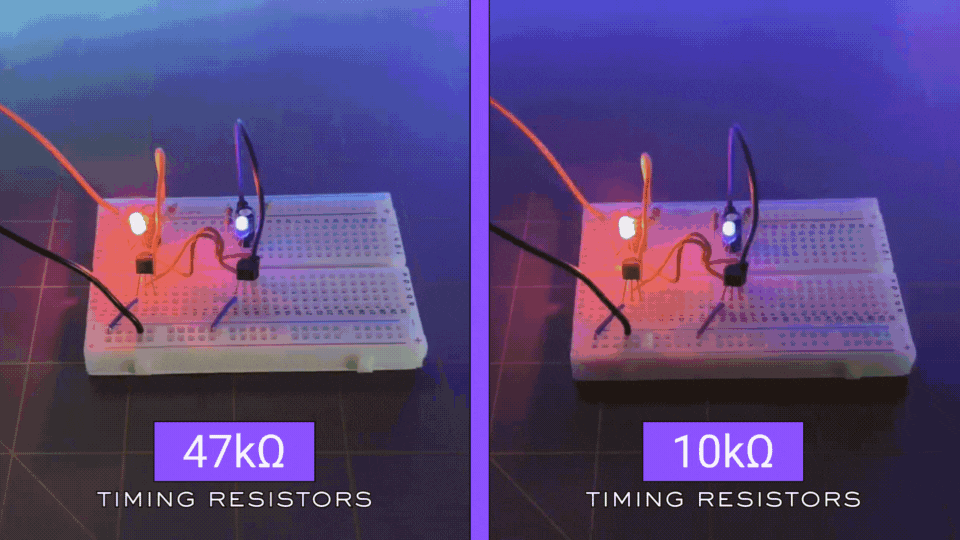
I tried using both 47kΩ and 10kΩ values for the timing resistors (resistors feeding the base). The following GIF image shows the difference in flash speed for each value for this circuit:
Where the Blinking Rate (Frequency) Comes From
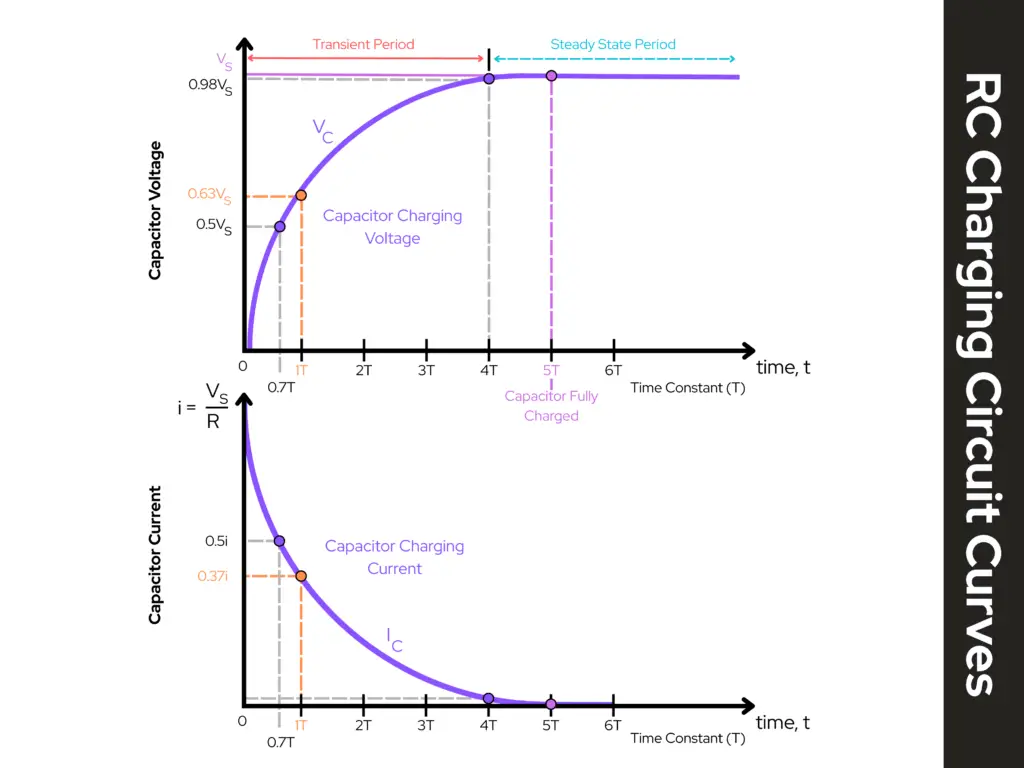
Recall from physics that to find the frequency we must know the period of a waveform. The period (T) of the wave is the time it takes for one oscillation to take place, or for one complete wavelength to pass a reference point. Period, being a time, is measured in units of time such as seconds, hours, days or years.
The period of a waveform is given by the formula:
\begin{equation}
T = \frac{1}{f}
\end{equation}
T is the period (measured in seconds [s]), and f is the frequency (measured in hertz [Hz])
The period of one complete blink cycle is approximately:
\begin{equation}
T \approx 1.4 \times R \times C
\end{equation}
This comes from the math behind RC charging curves:
- Each capacitor charges for about 0.7 × R × C seconds before a transistor switches
- There are two capacitors
- Therefore: 0.7 + 0.7 = 1.4
The blink frequency is:
\begin{equation}
f = \frac{1}{T} \approx \frac{1}{1.4RC}
\end{equation}
So in the LED blinker circuit:
- C1 = C2 = 10µF
- R3 = R4 = 47kΩ
- So, R×C = 0.47 seconds
- Full cycle ≈ 1.4 × 0.47 ≈ 0.66 seconds per full blink cycle (roughly 1.5 blinks per second per LED)
That’s why the red and blue LEDs of the LED blinker circuit flashes like classic patrol-car lights.

🤔 Where the 1.4 Comes From
Looking back at the period of one complete blink cycle from above, we saw that it was given by the product of the values of the resistor (R), the capacitor (C), and 1.4:
\begin{equation}
T \approx 1.4 \times R \times C
\end{equation}
But where did this value of 1.4 come from? It comes from the math of charging a capacitor through a resistor from one transistor’s turn-on threshold to the other.
More specifically, it’s approximately:
\begin{equation}
2 \times ln(2)
\end{equation}
which equals:
\begin{equation}
2 \times 0.693 \approx 1.386
\end{equation}
The value of 1.386 is rounded to 1.4.
But here’s what that actually means in real-circuit behavior: The astable’s timing is based on RC charging between two thresholds. Let’s talk about that next.
✌️ The Astable’s Timing is Based on RC Charging Between Two Thresholds
In a two-transistor astable (like ours), the timing is set by an RC network that is charging from a negative kick up to the base turn-on voltage (~0.6V). This ramping takes a predictable amount of time governed by the exponential charging curve:
\begin{equation}
V(t) = V_{final} \times (1 – e^{(\frac{-t}{RC})})
\end{equation}
The important thing is that the capacitor doesn’t charge all the way. It charges only from one threshold to another. The “distance” between those thresholds happens to be such that the timing works out to about 0.7 × R × C per half-cycle.
So the entire period is two half-cycles:
\begin{equation}
T \approx 2 \times (0.7 \times R \times C) \approx 1.4 \times R \times C
\end{equation}
And the blink frequency is:
\begin{equation}
f \approx \frac{1}{(1.4 \times R \times C)}
\end{equation}
That’s where the magic 1.4 comes from.
🤔 Why 0.7 × RC for each half-cycle?
This comes directly from the capacitor charging curve. The capacitor has to climb from a kicked low voltage up to the transistor’s base-emitter threshold (~0.6–0.7V) while the collector it’s referenced to is sitting at about 9V or 0V depending on state.
When you solve the exponential for the time needed to reach the threshold you get:
\begin{equation}
t \approx R \times C \times ln(2)
\end{equation}
Because ln(2) ≈ 0.693, we approximate this as:
\begin{equation}
t \approx 0.7 \times RC
\end{equation}
🤔 How Did You Solve the Exponential for the Time Needed to Reach the Threshold?
Remember, we have a two-transistor LED blinker, so the math isn’t random.
The One RC Fact We Start With
When a capacitor charges through a resistor toward some final voltage, the capacitor voltage follows an exponential curve:
\begin{equation}
V_{C}(t) = V_{F} + (V_{C}(0) – V_{F})e^{\frac{-t}{RC}}
\end{equation}
Where:
- VC(t) = capacitor voltage at time t
- VC(0) = capacitor voltage at t = 0 (starting voltage)
- VF = final voltage it’s charging toward (the “target” it would reach after a long time)
- R and C are the resistor and capacitor in the charging path
That’s the general form that always works.
The special case that produces t = RCln(2)
The famous t = RCln(2) comes from a very specific threshold condition:
The capacitor starts at 0V and we ask: “How long until it reaches half of its final value?”
That “halfway point” is what gives ln(2).
Step 1: Use the common simplified charging form
If the capacitor starts at 0V and charges toward VS (a supply or effective final voltage), the equation becomes:
\begin{equation}
V_{C}(t) = V_{S}(1 – e^{\frac{-t}{(RC)}})
\end{equation}
Step 2: Set the threshold to “half the final value”
Half the final value means:
\begin{equation}
V_{C}(t) = \frac{1}{2}V_{S}
\end{equation}
Substitute into the equation:
\begin{equation}
\frac{1}{2}V_{S} = V_{S}(1 – e^{\frac{-t}{(RC)}})
\end{equation}
Step 3: Divide both sides by VS
\begin{equation}
\frac{1}{2} = 1 – e^{\frac{-t}{(RC)}}
\end{equation}
Step 4: Move terms around
Subtract 1 from both sides:
\begin{equation}
\frac{1}{2} – 1 = -e^{\frac{-t}{(RC)}}
\end{equation}
\begin{equation}
-\frac{1}{2} = -e^{\frac{-t}{(RC)}}
\end{equation}
Multiply both sides by -1:
\begin{equation}
\frac{1}{2} = e^{\frac{-t}{(RC)}}
\end{equation}
Step 5: Take the natural log (ln) of both sides
\begin{equation}
ln(\frac{1}{2}) = ln(e^{\frac{-t}{(RC)}})
\end{equation}
The right side simplifies because ln(ex) = x:
\begin{equation}
ln(\frac{1}{2}) = \frac{-t}{(RC)}
\end{equation}
Step 6: Solve for t
Multiply both sides by –RC:
\begin{equation}
t = -RCln(\frac{1}{2})
\end{equation}
And here’s the identity:
\begin{equation}
\boxed{ln(\frac{1}{2}) = -ln(2)}
\end{equation}
So:
\begin{equation}
t = -RC(-ln(2)) = RCln(2)
\end{equation}
Step 7: Numerical value
\begin{equation}
ln(2) \approx 0.693
\end{equation}
So:
\begin{equation}
t \approx 0.693RC \approx \boxed{0.7RC}
\end{equation}
That’s exactly where “0.7 × RC” comes from.
🤔 Why multiply by 2?
Because the circuit alternates:
- When the red LED in ON, the blue LED in OFF
- When the blue LED in ON, the red LED is OFF
Each LED stays on for a “half-cycle,” but the full period is:
Red ON + Blue ON = two (0.7 × RC) intervals
So, the total period (T) is:
\begin{equation}
T \approx 2 \times (0.7 \times RC) = 1.4 \times RC
\end{equation}
And therefore, the frequency (f) is:
\begin{equation}
f = \frac{1}{T}
\end{equation}
\begin{equation}
f = \frac{1}{1.4 \times RC}
\end{equation}
⏱️ Recap of What Sets the Timing
The blink speed comes from the classic RC time constant:
- One half-cycle ≈ 0.7 × R × C
- Full cycle ≈ 1.4 × R × C
In our LED blinker circuit (astable multivibrator):
- R3 and R4 determine how fast the capacitors charge
- C1 and C2 determine how much charge is needed
- Together they decide how long before each transistor flips
- The bigger R or C is, the slower the blinking
- The smaller R or C is, the faster the blinking
This makes the astable incredibly easy to tune for the exact effect you want — including an old-school police-car wig-wag pattern, which our circuit can absolutely do.
Manipulating the Police-Car Wig-Wag Pattern of the Blinker Circuit
Back when we made the LED blinker circuit in How Components Work Together in Real Circuits, we used a red and a blue LED to create an effect that looked like flashing police lights. The blink rate we created was around 1.5 times per second.
How did we get this blink rate the way we wanted to? That’s what we’ll go through next. First thing we want to know though is, what the blink rate is we are aiming for? You can choose whatever blink rate you want to aim for — a slow blink rate or a fast blink rate — I chose for a nice steady rate I felt looked more closely to a police-car wig-wag pattern.

1. What blink rate are we aiming at?
Old-school alternating police-car flashers are roughly in the ballpark of about 1–2 blinks per second — meaning each LED blinks one-to-two times per second. So, each LED is on for around 0.25-0.5 seconds.
In a symmetric astable like our LED blinker circuit, each LED’s ON time is approximately:
\begin{equation}
0.7 \times R \times C
\end{equation}
Where the full cycle — the red LED goes ON, then the blue LED goes ON, then back to red again — is approximately:
\begin{equation}
1.4 \times R \times C
\end{equation}
So, the blink frequency is approximately:
\begin{equation}
\frac{1}{1.4 \times RC}
\end{equation}
Where R is the timing resistor and C is the timing capacitor for each side. We don’t have to be exact; we just pick RC values in the right range.
2. Concrete values to try (police-style wig-wag)
Let’s try a few different options to try to pin down the blink rate we want in keeping with the look of our LED flashes being more closely to a real police-car wig-wag pattern.
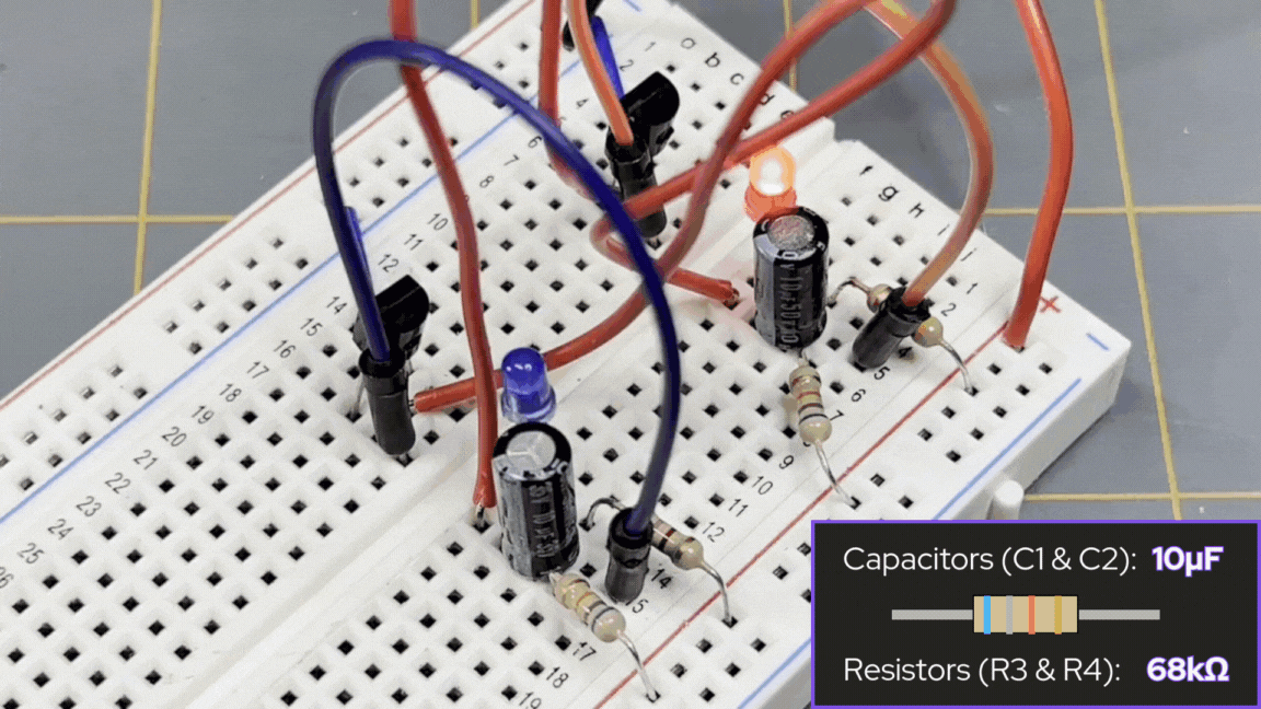
🐢 Option A – Slower, more deliberate (~1 blink/sec per LED)
Let’s say we start with using the following values for the capacitors and timing resistors (R3 and R4, as seen in the schematic diagram of the LED blinker circuit shared above):
- C1 = C2 = 10µF
- R3 = R4 = 68kΩ
Now, each LED ON time is approximately:
\begin{equation}
\approx 0.7 \times R \times C
\end{equation}
\begin{equation}
\approx 0.7 \times 68k\Omega \times 10\mu{F}
\end{equation}
\begin{equation}
\approx 0.7 \times 68,000\Omega \times (10\times10^{-6}F)
\end{equation}
\begin{equation}
\approx \boxed{0.48 \; \text{seconds}}
\end{equation}
For one full cycle (full period) — the red LED goes ON, then the blue LED goes ON, then back to red again — the ON time for both LEDs would be approximately:
\begin{equation}
\approx 1.4 \times R \times C
\end{equation}
\begin{equation}
\approx 1.4 \times 68k\Omega \times 10\mu{F}
\end{equation}
\begin{equation}
\approx 1.4 \times 68,000\Omega \times (10\times10^{-6}F)
\end{equation}
\begin{equation}
\approx \boxed{0.95 \; \text{seconds}}
\end{equation}
The blink rate or frequency of the LED blinker circuit would then be approximately:
\begin{equation}
\approx \frac{1}{1.4 \times RC}
\end{equation}
\begin{equation}
\approx \frac{1}{0.95 \; \text{seconds}}
\end{equation}
\begin{equation}
\approx \boxed{1 \; \text{Hz}}
\end{equation}
So, the blink rate for the LED blinker circuit — using 10µF capacitors for C1 and C2, and 68kΩ resistors for R3 and R4 — would give us a blink rate of about 1 hertz (Hz). More like a slow warning light than a frantic siren.
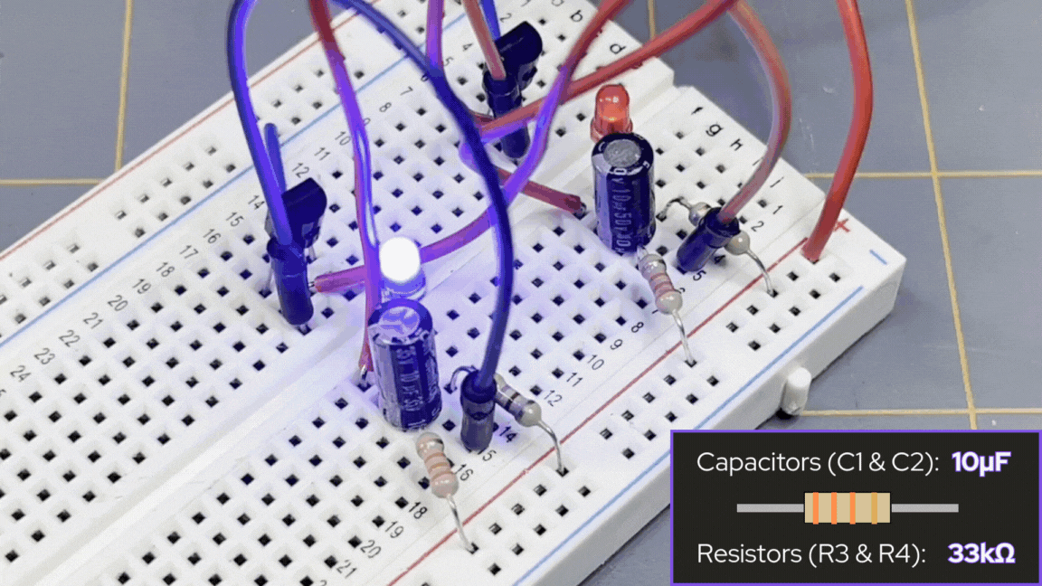
🐇 Option B – Slightly faster “urgent” flash (~2 blinks/sec per LED)
Let’s say we used the following values for the capacitors and timing resistors instead:
- C1 = C2 = 10µF
- R3 = R4 = 33kΩ
This means that:
- Each LED ON time ≈ 0.7 × 33kΩ × 10µF ≈ 0.23 seconds
- Full period ≈ 1.4 × 33kΩ × 10µF ≈ 0.46 seconds
- Blink rate ≈ 1/1.4 × R × C ≈ 1/0.46s ≈ 2.2 Hz
This will look more like a modern “urgent” flasher — snappier, still very readable.
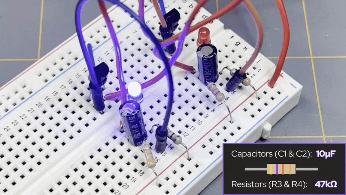
🎯 Option C – “Classic wig-wag” (~1–1.5 blinks/sec per LED)
Now, let’s take a look at the values for the capacitors and timing resistors we actually used in our LED blinker circuit from How Components Work Together in Real Circuits:
- C1 = C2 = 10µF
- R3 = R4 = 47kΩ
This means that:
- Each LED ON time ≈ 0.7 × 47kΩ × 10µF ≈ 0.33 seconds
- Full period ≈ 1.4 × 47kΩ × 10µF ≈ 0.66 seconds
- Blink rate ≈ 1/1.4 × R × C ≈ 1/0.66s ≈ 1.5 Hz
This feels very much like an old patrol car: solid, obvious, not too frantic.
3. Alternate way: keep your resistors, change the caps
If you’d rather leave resistors alone and only swap capacitors, then you can do that.
🐢🐢 Option W – Way too slow
Say your timing resistors (R3 and R4) are both 47kΩ right now. Now let’s say capacitors C1 and C2 are now 680µF, then the ON time for each LED would be approximately:
- C1 = C2 = 680µF
- R3 = R4 = 47kΩ
Each LED ON time ≈ 0.7 × 47kΩ × 680µF ≈ 22 seconds
Full period ≈ 1.4 × 47kΩ × 680µF ≈ 45 seconds
Blink rate ≈ 1/66s ≈ 0.02 Hz
This is way too slow! That’s a period getting close to lasting almost a full minute! It’s so slow the police-car lost its wig-wag and went straight to red and blue mood lighting.
I didn’t have any 680µF capacitors to demonstrate in an example GIF image for this one. Sorry 😕.
🐢 Option X – Still too slow
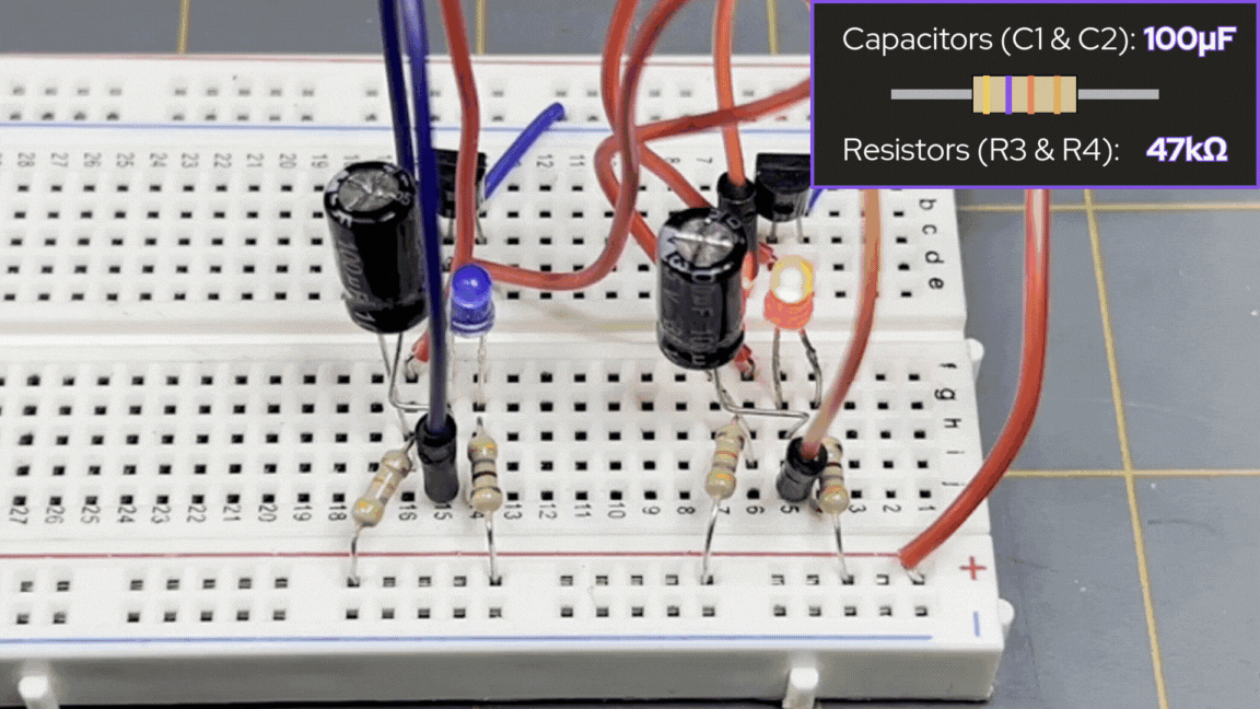
Say your timing resistors (R3 and R4) are both 47kΩ right now. Now let’s say capacitors C1 and C2 are now 100µF, then the ON time for each LED would be approximately:
- C1 = C2 = 100µF
- R3 = R4 = 47kΩ
Each LED ON time ≈ 0.7 × 47kΩ × 100µF ≈ 3.3 seconds
Full period ≈ 1.4 × 47kΩ × 100µF ≈ 6.6 seconds
Blink rate ≈ 1/6.6s ≈ 0.2 Hz
This is still too slow — so slow your turn signal would be a better emergency flasher.
🐇 Option Y – Too fast
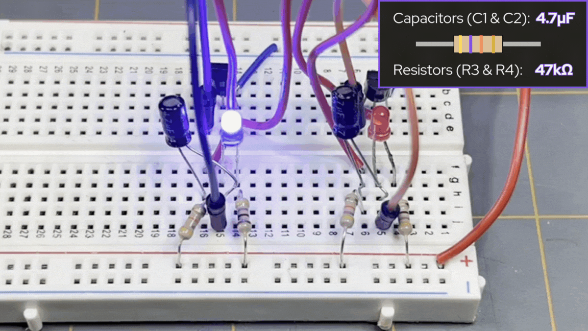
Keeping the timing resistors (R3 and R4) both at 47kΩ, let’s say we changed the value of the capacitors (C1 and C2) to 4.7µF instead:
- C1 = C2 = 4.7µF
- R3 = R4 = 47kΩ
Each LED ON time ≈ 0.7 × 47kΩ × 4.7µF ≈ 0.15 seconds
Full period ≈ 1.4 × 47kΩ × 4.7µF ≈ 0.3 seconds
Blink rate ≈ 1/0.3s ≈ 3.3 Hz
This speed is too fast and gives a bit more of an urgent look than what Option B gave us before.
🎯 Option Z – Just right
Keeping the timing resistors (R3 and R4) both at 47kΩ, let’s say we changed the value of the capacitors (C1 and C2) to 10µF instead:
- C1 = C2 = 10µF
- R3 = R4 = 47kΩ
Each LED ON time ≈ 0.7 × 47kΩ × 10µF ≈ 0.33 seconds
Full period ≈ 1.4 × 47kΩ × 10µF ≈ 0.66 seconds
Blink rate ≈ 1/0.66s ≈ 1.5 Hz
This is the exact same setup we had for Option C above, where we get the feel of an old patrol car for the blink rate of our LEDs.
🎯 So What Values Should You Change for Police-Car Blink Speed?
Remember what we said, the timing is controlled ONLY by the capacitors (C1 and C2) and the resistors (R3 and R4), as shown in the schematic diagram of the LED blinker circuit shared above.
These form the RC network that determines how quickly each transistor’s base voltage ramps up. So to set the blink speed, you tune R3 and R4 and/or C1 and C2. NOT the LED resistors. The LED resistors just control brightness.
🚔 Recommended Police-Car Timing Values
To get approximately 1.5–2 flashes per second per LED — the classic wig-wag look — use the following options and their values:
Option 1 — Keep C1 and C2 the same, and change R3 and R4 only
- C1 = C2 = 10µF
- R3 = R4 =47kΩ
This gives approximately 0.33 seconds per LED. This gives a clean alternate flashing look that has a very authentic rhythm.
If you want it a bit faster, then change both resistor values to 33kΩ. If you want slower, then change both resistor values to 56-68kΩ.
Option 2 — Keep R3 and R4 the same, and change C1 and C2 only
If R3 and R4 are currently 47kΩ, then with a value of 100µF for both C1 and C2 should give a blink that is slow (about 3 seconds per LED).
If you use a value of 4.7µF for both capacitors (C1 and C2), and leave R3 and R4 at 47kΩ, then this gives a blink rate that’s sped up a bit — might not be what we’re looking for.
If you were to use:
- C1 = C2 = 10µF
- R3 = R4 =47kΩ
This gives the right blink rate for that police-car vibe.
🔍 Why These Parts Matter
Resistors R3 and R4 build the base drive paths that:
- Feed the opposite transistor
- Charge through the timing capacitors
- Set the time constant τ = R × C
Capacitors C1 and C2 provide the timing that:
- Pass the “kick” that switches states
- Slowly charge through R3/R4
- Determine how long until the next flip
The LED resistors have no effect on timing — they’re purely current limiters for the LEDs.
Summary for the Blinker LED Circuit
This subseries on astable multivibrators was meant to be a companion to the Circuit Component Super Series — specifically, as an extended topic for the LED Blinker Circuit we made in Part 3 of the component series titled, “How Components Work Together in Real Circuits: Having Components Join Forces.” The LED blinker circuit we’ve used along for each of these extended discussion topics used the following components:
- 4 resistors total, no collector pull-up resistors
- Timing resistors (R3 and R4)
- LED resistors (R1 and R2)
- Timing was set by resistors R3 and R4, as well as the capacitors C1 and C2
When we built the LED blinker circuit, we recognized that we had set the blink rate of the LEDs to have a rhythm similar to an old-school police-style alternate flashes, which was really cool. To achieve this look, we used the following values:
- C1 = C2 = 10µF
- R3 = R4 =47kΩ
Using these values gave us the sweet spot for the right kind of flash we wanted for our po-po lights. To see what this circuit looks like, you can view the schematic diagram of the LED blinker circuit shared above. To build this circuit yourself, you can check out how to at our page titled, “How Components Work Together in Real Circuits: Having Components Join Forces.”
If you’re more of a visual learner, you can see the video build of the LED blinker circuit here.
What’s Next
Now that you have a much better understanding of astable multivibrators and the LED blinker circuit we made, you can now continue on from here in our Circuit Component Super Series, where the next order of business is when we go from schematic to breadboard and build ourselves another circuit — that’ll be Part 4 of our 12 Part Super Series on Electronic Components.
If you’re eagerly waiting to know when the next installment of our super series is to arrive, or are interested in knowing about other things happening here at Motbots, join our newsletter! If you’re signed up to the newsletter, you’ll be kept up-to-date on new topics of discussion, video content, projects and more! We promise not to get spammy and bother you too much 😁.
We want to send our appreciation by thanking you for coming to visit our site and participate in the content we provide here for you. We genuinely hope that you have found this content acceptable, useful, and educational. We’d love to hear from you! Leave us a comment below and let us know what you think!
Thank you and remember to keep at it and stay motivated.
