Introduction to PIC Programming Using C: Byte Lights With the ADC – Part 1: The ADC
Introduction
Welcome! In the following parts of this series, our goal is to understand analog-to-digital conversion (ADC) of a PIC microcontroller, and how to program one to accept and convert an analog input.
It is my personal goal to help guide you to do this in a way that I learned from a terrific book I purchased some time ago of which you can observe for yourself at the Book Reference at the bottom of this page.
The following is intended to be an enhancement to such pedagogical material that sometimes leaves more to be desired for the reader. It is the intention of the following to add more input to the learning material that is currently available, or currently unavailable, in the market today on learning how to program a PIC microcontroller using the C programming language.
Goal of This Project Series
The goal of this project series is to get us familiar with the ADC of a PIC microcontroller. We will begin this series with a discussion of what ADC means, what the difference is between analog and digital signals, then we’ll move on to learn how a PIC is set up to use analog inputs.
Later in this series, we’ll apply what we’ve learned to build a circuit with 8 LEDs that visually represent a digital binary value corresponding to an analog input signal — controlled by a variable voltage from a potentiometer, as shown in the example circuit below:
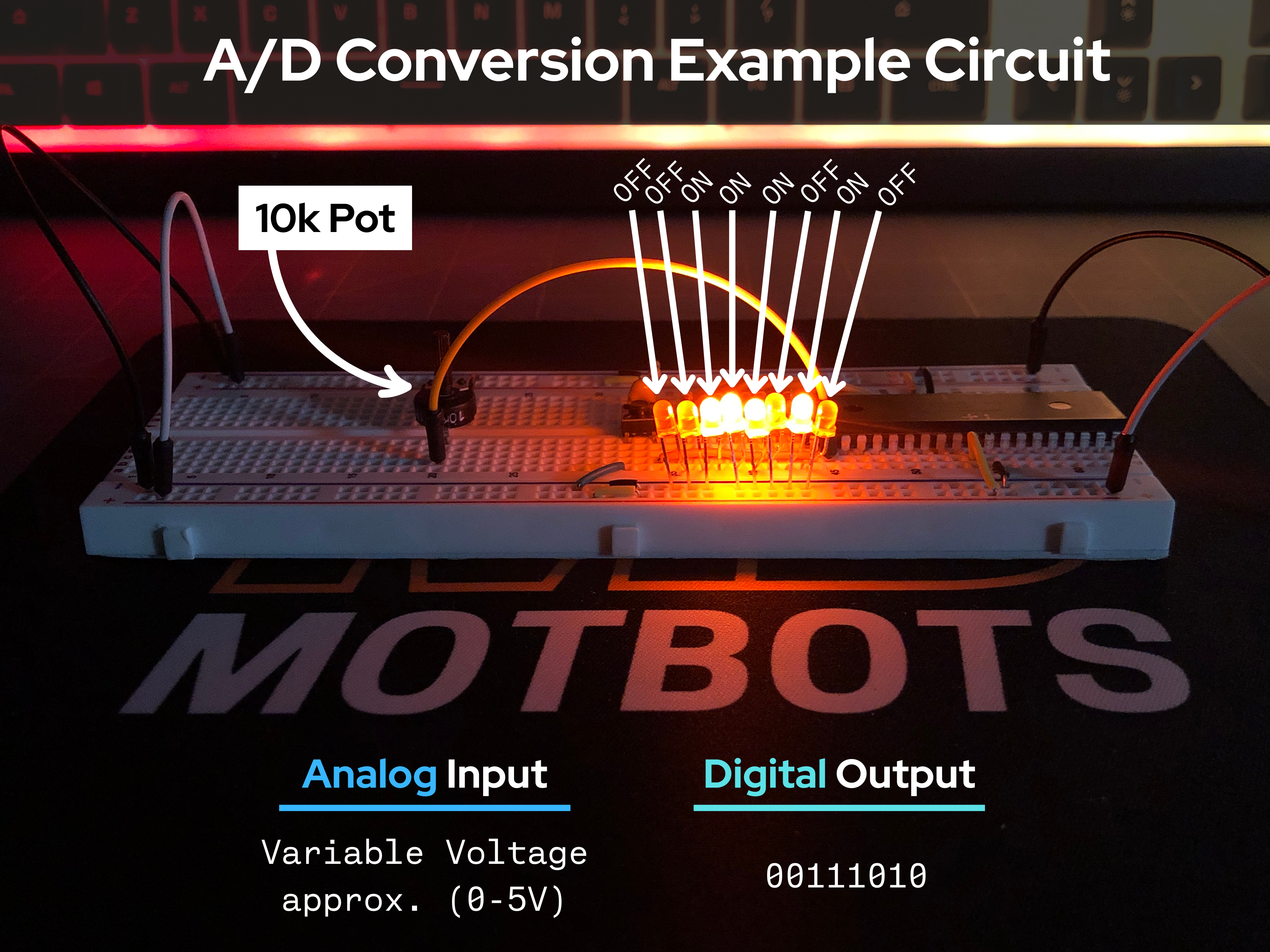

In short, the prototype circuit will:
- Accept an analog variable voltage signal that is sourced through a potentiometer.
- That analog signal will be converted to a digital signal.
- That digital signal will be processed and output through 8 pins to 8 corresponding LEDs in the circuit that will provide a sequence of binary values telling each of those LEDs to either be turned on or off. This will give a visual representation of the analog input value in an illuminated digital binary form.
Three Part Series Sequence:
- Part 1: The ADC – Here, we learn about analog-to-digital conversion of a PIC microcontroller.
- Part 2: The Mock-Up – This is when we will build a mock-up circuit consisting of 8 LEDs that will provide a visual binary output of an analog input coming from a variable voltage signal through a potentiometer.
- Part 3: The Code – At this stage, we’ll walk through the code that sets up the PIC18F4525 microcontroller to read a single analog input and output 8 digital signals — lighting up LEDs to visually represent the variable input voltage.

The PIC18F4525 Datasheet
For this learning series, we’ll be using Microchip’s PIC18F4525 microcontroller. It’s highly recommended that you download and observe the provided datasheet below for the PIC18F4525.
We will be using the datasheet to thoroughly go over our topic of discussion here, and in future parts of this series. The datasheet is where we will find the information that we need to program the PIC.
Microchip PIC18F4525 Datasheet
Download the PIC18F4525 Datasheet
What’s Analog-to-Digital Conversion?
The phrase “analog-to-digital conversion” is used to describe a process of capturing an electric analog signal and converting it into a series of numeric digital values. This electronic device is known to be the A/D or ADC, which are the acronyms used to represent an Analog-to-Digital Converter.
Digital vs. Analog Inputs
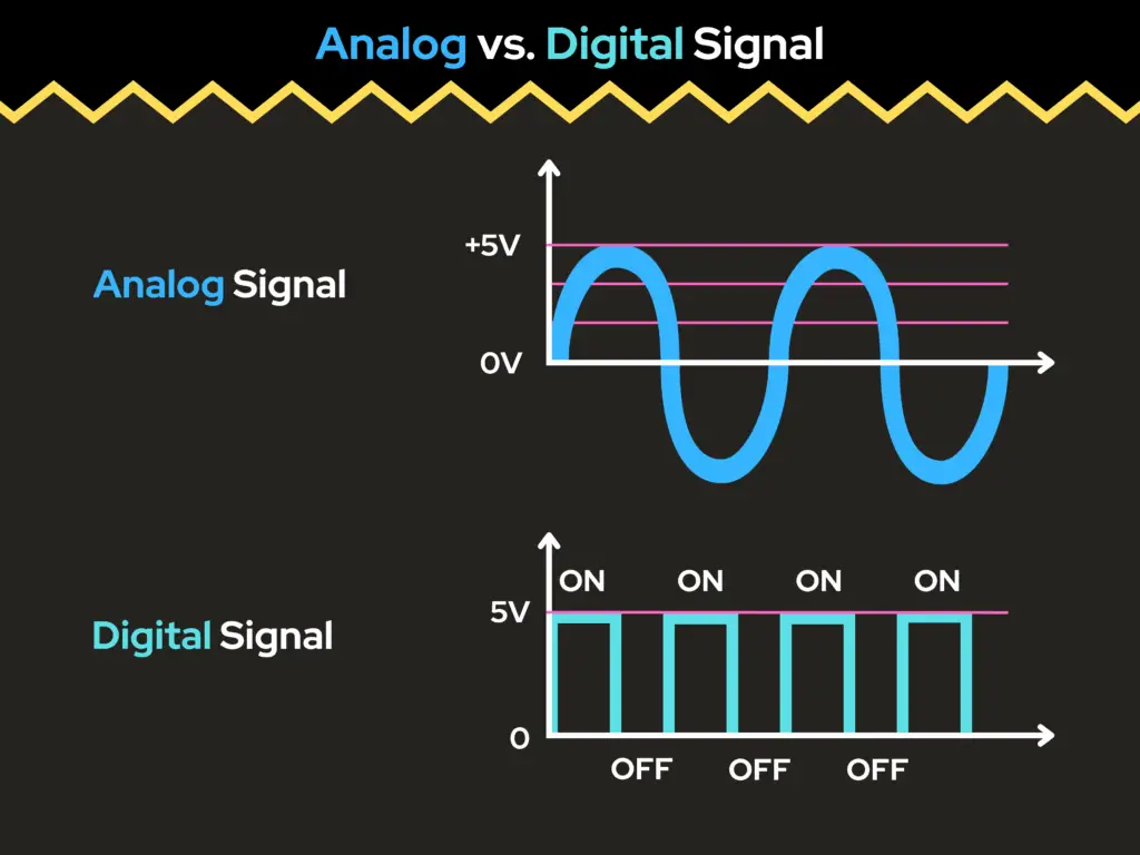
Analog and digital input signals are two fundamental types of signals used in electronics to convey information. Analog inputs handle continuous signals that can take on a range of values, whereas digital inputs handle discrete signals that have only two states: ON (1) or OFF (0).
When working with PIC microcontrollers, understanding the difference between analog and digital inputs is essential because each serves a different purpose in interfacing with the real world. Let’s begin our discussion with a deeper understanding of the differences between digital and analog input signals, then we’ll move on to how we can use an analog input and configure a Microchip PIC18F4525 microcontroller (MCU) to do so.
Digital Inputs
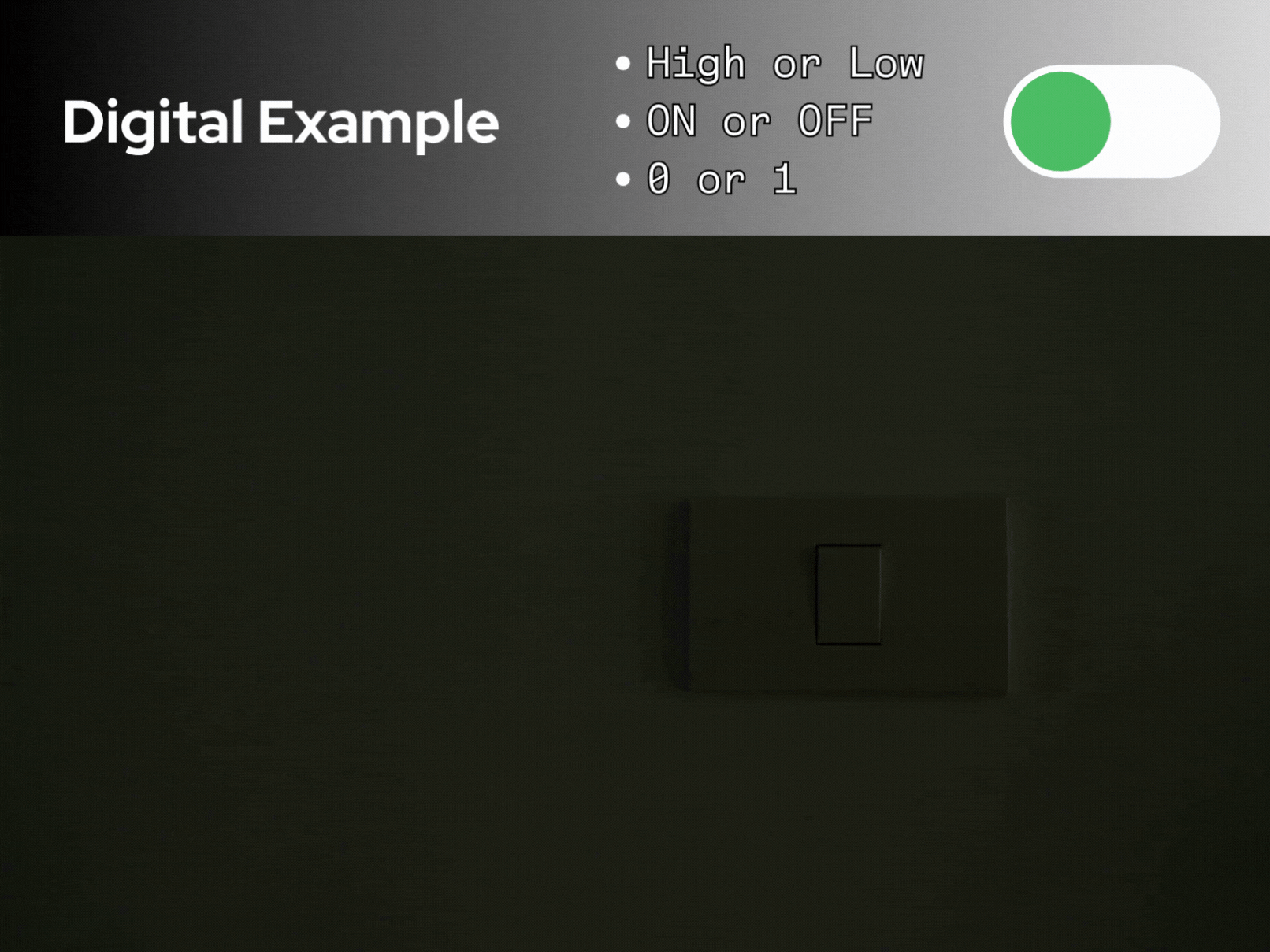
Digital inputs are binary in nature – they can be of either two states:
- High or Low
- 0 or 1
- ON or OFF
- 0V or 5V
Examples of digital input sources are things like a push-button switch, digital sensors, and motion detectors, to name a few. These are items used when you care to know if something is on or off, for example, or when something has been activated or not.
The main concern about a digital input on a device is whether the input signal is either on or off, its voltage reading is either high or low, or the input signal is either a logic 0 or a logic 1.
Analog Inputs
Analog inputs can ideally take up any continuous range of voltages, as in between 0 volts and 5 volts, for example. Instead of just two states, they can be of any value within the given range, such as:
- 0V
- 1.5V
- 3.3V
- 5V
Examples of analog input sources are things like potentiometers, temperature sensors, and light sensors, to name a few. Such an example is a dimmer switch or potentiometer that can vary the voltage input, therefore changing the intensity of the light being output from a light source.

Common Types of Analog Inputs
- Voltage Input
- Signal Range: Typically 0-5V, 0-10V, ±5V, or ±10V
- Features:
- Directly measures voltage
- Weak noise protection
- Vulnerable to interference over long-distance transmission
- Example Devices:
- Potentiometers
- Temperature sensors
- Current Input
- Signal Range: Typically 4-20mA, or 0-20mA, is an industrial standard
- Features:
- Strong noise protection
- Capable of long-distance transmission
- A precise external resistor is necessary to transform the signal into a measurable voltage for the ADC.
- Example Devices:
- Humidity sensors
- Infrared detectors
- Resistance Input:
- Measurement Method: Resistance is measured through either constant current excitation or by using a voltage divider.
- Example Sensors:
- Resistance Temperature Detector (RTD): A temperature sensor known for its consistent and linear response.
- Thermistors (NTC/PTC): Due to their nonlinear characteristics, temperature must be calculated using equations or data tables.
- Strain Gauge: A sensor for force or pressure that requires a Wheatstone bridge for signal conversion.
Summary Table of Analog and Digital Inputs
| Feature | Digital Input | Analog Input |
| Signal Type | ON/OFF (binary) | Range of voltages (continuous) |
| Typical Voltage | 0V or 5V | 0V to 5V (whatever VREF is) |
| Input Pins | General I/O pins | Analog specific (ANx) pins |
| Processing Needed | No conversion needed | Needs ADC conversion |
| PIC Usage | PORTx | ADCON0, ADRESH: ADRESL |
Using Analog Inputs
Typical voltage ranges for PIC microcontrollers are between 0V and 5V. Voltage values within such a range are ideal because the voltage will increase in discrete steps based on the resolution of the analog-digital converter (ADC).
Why You Want to Calculate or Know ADC Resolution
We’ll get into what the resolution is in a moment, after we learn to make the calculation for it. First, let’s get into why we want to find the resolution. The reason why we want to know the resolution is because it tells us how precisely the microcontroller can measure an analog voltage.
An example of why we might need to know the resolution would be to understand measurement precision to match sensor accuracy.
- If you’re using sensors (like temperature sensors, pressure sensors, etc.), you need to make sure the ADC resolution is at least as fine as the changes you want to detect.
- Example: A temperature sensor that changes 10 mV per °C — if your ADC resolution is 5 mV/step, then each ADC step corresponds to 0.5 °C, which might or might not be acceptable based on your needs.
Finding the Resolution of the PIC18F4525
The resolution of the ADC can be determined by performing the following calculation:
\begin{equation}
\text{Resolution} = \frac{\text{Range}}{2^{n}}
\end{equation}
So, if we put in place what the definition of the range is into this equation, the ADC resolution is now given by the following formula:
\begin{equation}
\text{Resolution} = \frac{V_{REF+} – V_{REF-}}{2^{n}}
\end{equation}
Where:
- VREF+ is the positive voltage reference (usually tied to VDD, e.g., 5V)
- VREF- is the negative voltage reference (usually tied to VSS or GND, 0V)
- n is the number of ADC bits (10 bits for the PIC18F4525, as given on pg. 223, under section 19.0 of the datasheet)
- 2n = 1024 steps (where n = 10, for the 10-bit ADC)
The range and resolution, then becomes:
\begin{equation}
\text{Range} = V_{REF+} – V_{REF-} = 5V – 0V = 5V
\end{equation}
\begin{equation}
\text{Resolution} = \frac{(5V)}{2^{10}} = \frac{(5V)}{1024} = \boxed{4.88mV}
\end{equation}
The resolution of the ADC tells us the smallest change in voltage it can detect. For the PIC18F4525, using a 10-bit ADC with a 0–5V reference range, this resolution is approximately 4.88 millivolts per step.
This means that if we enable the analog input functionality on the appropriate pins, the smallest voltage difference the ADC can “see” is about 4.88 mV. In other words, within the 0 to 5V range, the ADC can only register voltages in 4.88 mV increments. So if the input voltage changes by less than this amount, the ADC may not detect it.
For example, the ADC will recognize:
- 0.000 V
- 0.00488 V
- 0.00976 V
- 0.01464 V
- … and so on, up to just under 5V.
As you can see, the PIC can’t detect every possible voltage in the range — because there are infinitely many real numbers between 0 and 5V. Instead, it can only detect a finite number of discrete voltage levels, determined by its resolution. In this case, the 10-bit ADC divides the 5V range into 1024 steps, each 4.88 mV apart.
Even though these increments are small, they’re often precise enough for most applications. Starting from 0V and increasing by 4.88 mV per step over 1024 steps brings us to a maximum measurable voltage of:
\begin{equation}
(1023)\;*\;(0.00488V) = 4.99712V
\end{equation}
This is effectively the upper limit of the ADC’s measurable range, just below 5V.
The principle behind the ADC operation in the PIC18F4525 is that there is a single ADC module inside the chip. This module can be switched (or multiplexed) between multiple input channels. In the case of the 40-pin PIC18F4525, there are up to 13 analog input channels that can be connected to the ADC. This technique — called multiplexing — allows one ADC to serve multiple analog inputs, one at a time.
If you’d like to learn more about the ADC of a PIC microcontroller, I encourage you to check out our discussion on The ADC (Analog-to-Digital Converter), on Part 3 of the Introduction to PIC Programming Using C: Programming a Super Simple LED Switch series. There, we mentioned that the ADC of the PIC18F4525 is controlled by three control registers: ADCON0, ADCON1, and ADCON2. We’ll talk more about the ADCON registers, next.

How the ADCON Registers Tie Into Using Analog Inputs
When you’re using analog inputs on the PIC18F4525, you’re telling the PIC, “I want to read a continuous (analog) voltage on one or more of these pins and convert it into a digital value I can use in my program.”
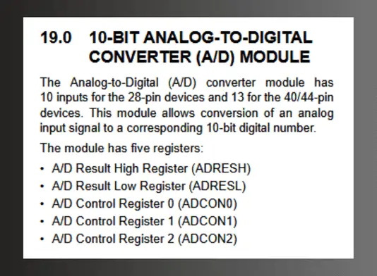
The ADC of the PIC18F4525 is controlled by three control registers:
- ADCON0: this register is primarily responsible for enabling the ADC and for which bit or channel the ADC is connected to.
- ADCON1: this register configures the voltage reference (e.g. VDD, VSS, or external) and the function to decide if the bit on the port is analog or digital.
- ADCON2: controls the timing of the ADC.
So, a step-by-step breakdown of what we’d need to do, as programmers, to configure the ADC using the control registers would be the following:
- Select the Analog Channel and Turn on the ADC → ADCON0
- Enable Analog Inputs and Select Reference Voltages → ADCON1
- Set the Acquisition Time, ADC Clock, and Result Format → ADCON2
What we do to setup and use the ADC of the PIC is to configure each of these control registers to their proper settings, according to how we want to use them. By selecting the bit values for each 8 bit register — each bit being either a logic ‘0’ or a logic ‘1’ — we can start a conversion and read a result. This process is shown in the image below:
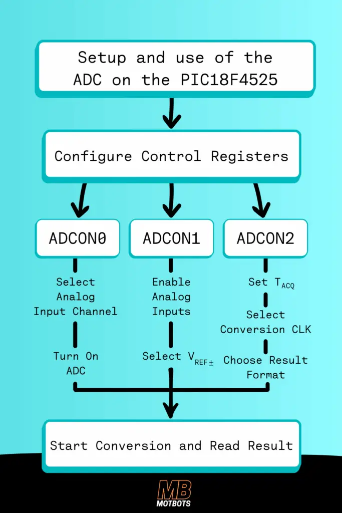
Now that we have a general idea of what the ADCONs are and what they do, let’s walk through what we need to do, as programmers, to set up each control register to use an analog input. We’ll start with the ADCON0 control register.
The ADCON0 Control Register
The ADCON0 control register is used to select which analog input channel is connected to the ADC. This process is a type of multiplexing, where multiple inputs are directed to a single device, one at a time.
- Only one analog input channel can be connected to the ADC at a time — the ADC uses multiplexing.
- You must select which analog input (e.g., AN0, AN1, etc.) you’re reading from.
Looking at the PIC18F4525 datasheet on pg. 223, for ADCON0, we can set the choices we have to control the data in the following bits:
ADCON0:
- bit 7-6: Unimplemented: Read as ‘0’
- bit 5-2: Analog Channel Select bits
- bit 1: A/D Conversion Status bit
- bit 0: A/D On bit
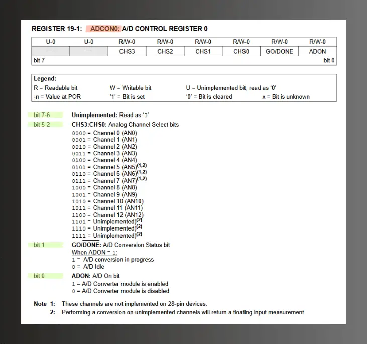
Let’s thoroughly walk through how we are to set the bits for the ADCON0 control register for our purpose of setting up the PIC for using an analog input:
- Bits 7 and 6 are unimplemented, so they are both to be read as a logic ‘0’. We will set both bits to a logic ‘0’.
- Bits 5, 4, 3, and 2, are all for setting the analog channel select. If we look at the PIC18F4525 datasheet on pg. 223, for ADCON0, we see that there are bit selection configuration options we could choose from to implement a number of channels of our preference (AN0 to AN12), as well as a few bit configuration options for these four bits to be unimplemented. We will set each bit here to a logic ‘0’, for the choice of Analog Channel 0 (AN0).
- Bit 1 is used to control the status of the ADC conversion, which tells the programmer when the conversion is finished. If needed, the programmer can set bit 1 to logic ‘1’ to start the ADC conversion. When the conversion is done, the microprocessor automatically sets bit 1 back to a logic ‘0’ – the signal that let’s the programmer know that the conversion is done. We will set this bit to a logic ‘0’, to set the A/D to idle.
- Bit 0 turns the ADC on or off – setting bit 0 as a logic ‘0’ disables the ADC, or setting bit 0 to logic ‘1’ enables the ADC. We will set this bit to a logic ‘1’, to enable the ADC.
The following instruction in code will set the ADCON0 control register the way we have just described above:
\begin{equation}
\text{ADCON0} = 0x01;
\end{equation}
The “0x” prefix in the address 0x01, stands for hexadecimal. We have to write a hexadecimal value this way. We could also represent the ADCON0 as a binary value equivalent to the hexadecimal value:
\begin{equation}
\text{ADCON0} = 0b00000001;
\end{equation}
The “0b” prefix in the address 0b00000001, stands for binary. We have to write a binary value this way. If you’re ever in a jam and needing to know the conversions of something like going from binary-to-hexadecimal to write out your code value as we did above, you can visit our simple Hexadecimal-Binary-Decimal Unit Conversion calculator here. Just know that the binary value 0b00000001 (0001) is equivalent to the hexadecimal value 0x01 (1).

The ADCON1 Control Register
The ADCON1 control register is used to control whether the 13 inputs are to be used as analog or digital. We need to configure the ADCON1 to enable the analog inputs and select the reference voltages.
- PIC I/O pins can be analog or digital. You must configure them for analog mode if you’re using them for ADC.
- Also, the voltage reference range affects resolution.
Looking at the PIC18F4525 datasheet on pg. 224, for ADCON1, we can set the choices we have to control the data in the following bits:
ADCON1:
- bit 7-6: Unimplemented: Read as ‘0’
- bit 5: Voltage Reference Configuration bit (VREF- source)
- bit 4: Voltage Reference Configuration bit (VREF+ source)
- bit 3-0: A/D Port Configuration Control bits
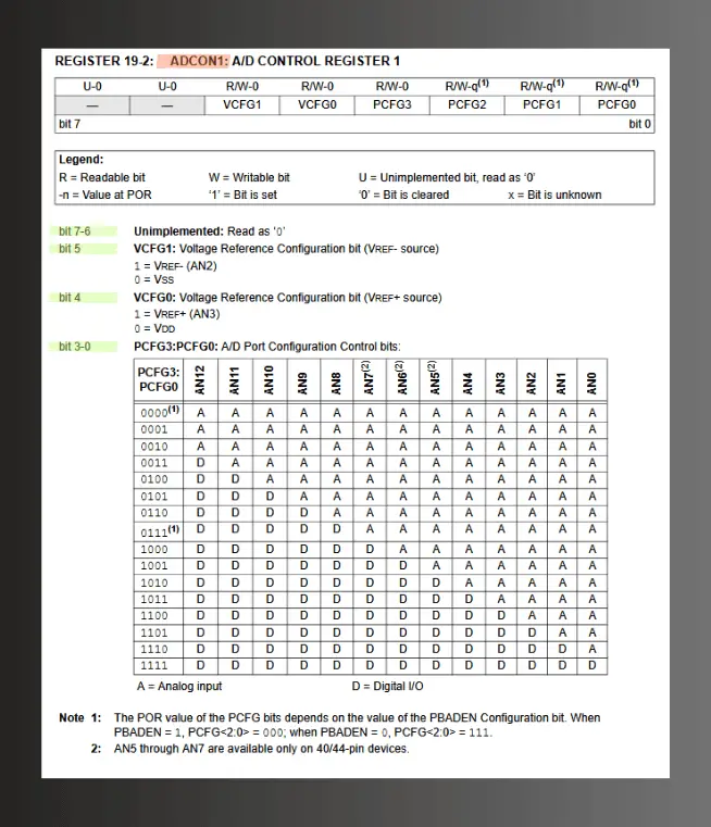
Let’s thoroughly walk through how we are to set the bits for the ADCON1 control register for our purpose of setting up the PIC for using an analog input:
- Bits 7 and 6 are unimplemented, so they are both to be read as a logic ‘0’. We will set both bits to a logic ‘0’.
- Bit 5 is to set the negative voltage reference, which is usually tied to VSS or GND — i.e. the 0V reference. We will set this bit to a logic ‘0’, for the VSS reference.
- Bit 4 is to set the positive voltage reference, which is usually tied to VDD — i.e. the 5V reference of the PIC. We will set this bit to a logic ‘0’, for the VDD reference.
- Bits 3, 2, 1, and 0, are all for setting the port configuration control. These are the bits we use to control which channels (AN0 to AN12) are to be analog or digital — i.e. whether the 13 inputs are to be used as analog or digital. In our case, we want to set all the bits to a logic ‘1’, to make them digital, except the last bit for channel AN0, where we’ll set it to a logic ‘0’, to make it analog.
The reason why we are setting bits 3, 2, and 1 to logic ‘1’, and bit 0 to logic ‘0’, to make only channel AN0 as an analog input is because we only want just one analog input (from a potentiometer we’ll use, later), and the rest of the pins free for digital I/O (the 8 LEDs we’ll use later for our prototype circuit).
Why Not Just Make All ANx Pins Analog?
The main reason to set only the channels you need as analog is because that’s all you need — setting each bit 3, 2, 1, and 0, to logic ‘0’ might cause problems or limit your flexibility. Here’s some reasons why setting all the channels (AN0 to AN12) as analog inputs is not ideal:
- Lost Digital I/O Capability: If you set all pins to analog mode:
- Those pins no longer behave like normal digital inputs or outputs (no logic HIGH/LOW reads/writes).
- If you try to use them in your code for digital purposes (LEDs, switches, etc.), it won’t work as expected.
- Floating Voltages/Power Waste: Unused analog inputs that aren’t tied to anything can float:
- This leads to unstable ADC readings.
- It may cause slight power consumption increases or electrical noise.
So, it’s best practice to avoid enabling analog mode on pins you don’t intend to use that way — and in our case, we only intend to use one analog input device for channel AN0.
The following instruction in code will set the ADCON1 control register the way we have just described above:
\begin{equation}
\text{ADCON1} = 0b00001110;
\end{equation}
We could also represent the ADCON1 as a hexadecimal value equivalent to the binary value:
\begin{equation}
\text{ADCON1} = 0x0E;
\end{equation}
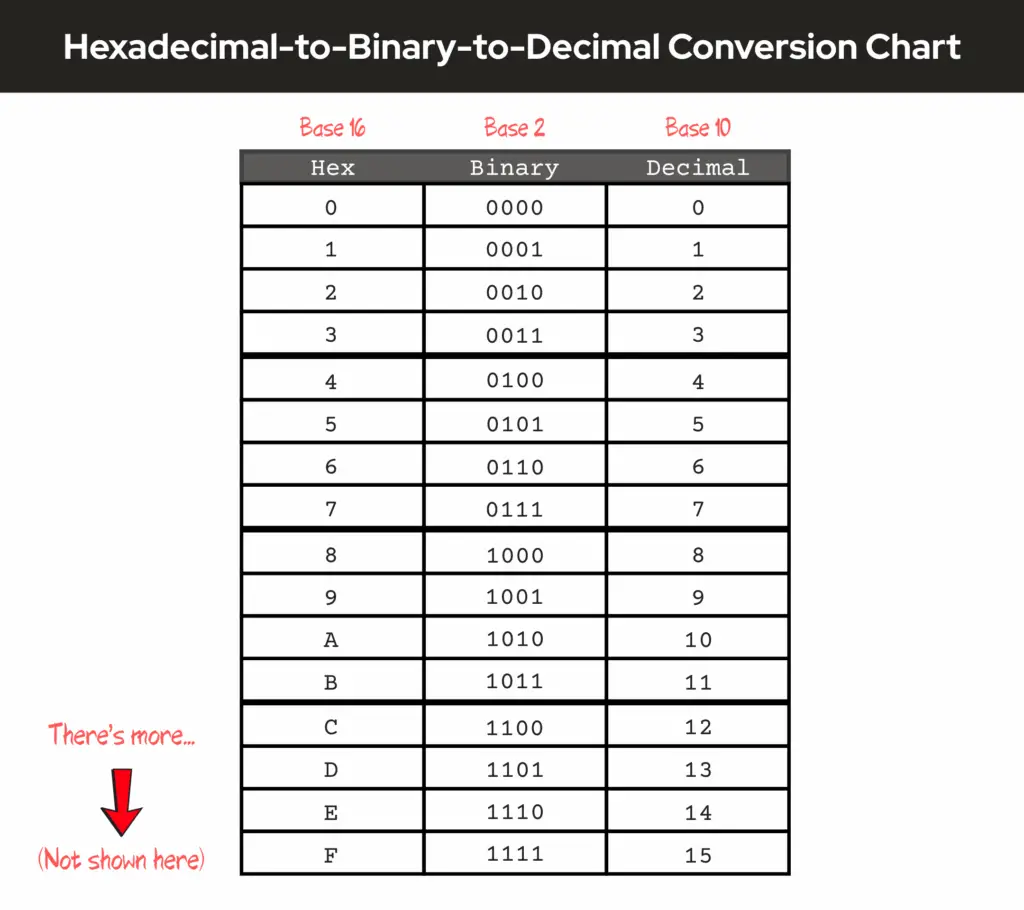
If you need to, you can visit our simple Hexadecimal-Binary-Decimal Unit Conversion calculator here, to see what the binary-to-hexadecimal conversion is. Just know that the binary value 0b00001110 is equivalent to the hexadecimal value 0x0E. Below is a hexadecimal-to-binary-to-decimal chart as a reference:
The ADCON2 Control Register
The ADCON2 control register use is threefold:
- It controls the A/D (Analog/Digital) conversion clock source or how fast the ADC converts.
- It controls the acquisition time or time to allow voltage to stabilize before conversion.
- It controls the result format, or the left or right-justification of the combination of bits between the two address registers, ADRESH and ADRESL.
Let’s first go over how the ADCON2 control register is used to decide what format the result of the ADC is stored in.
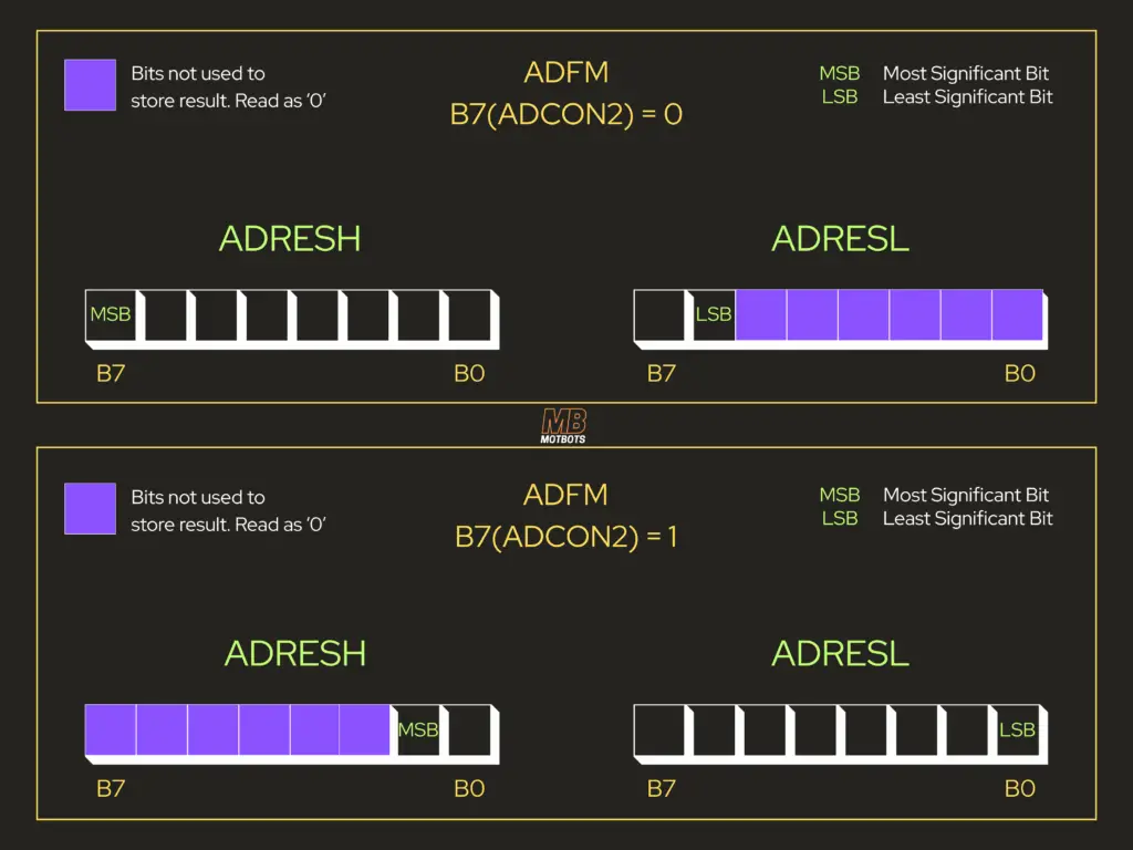
ADCON2 Result Format
The ADCON2 control register uses a result format because the ADC returns a 10-bit binary number. Remember, the PIC18F4525 MCU allows conversion of an analog input signal to a corresponding 10-bit digital number, as stated on pg. 223, under section 19.0 of the datasheet. So, the ADC returns a 10-bit binary number as the result of a conversion.
The thing though, is that the PIC18F4525 is an 8-bit PIC, which means each of its registers contain only 8-bits — uh oh. 😬
No problem though — this just means that the PIC needs to use two registers to store the result, and those two registers are: ADRESH and ADRESL — address high and address low. So, that would mean that 8 bits of the result would have to be stored in one register and the other 2 bits would have to be stored in the other register.
Looking at the PIC18F4525 datasheet on pg. 225, for ADCON2, we can set the choices we have to control the data in the following bits:
ADCON2:
- bit 7: ADFM: Is the A/D Result Format Select bit
- bit 6: Unimplemented: Read as ‘0’
- bit 5-3: ACQT2:ACQT0: A/D Acquisition Time Select bits
- bit 2-0: ADCS2:ADCS0: A/D Conversion Clock Select bits
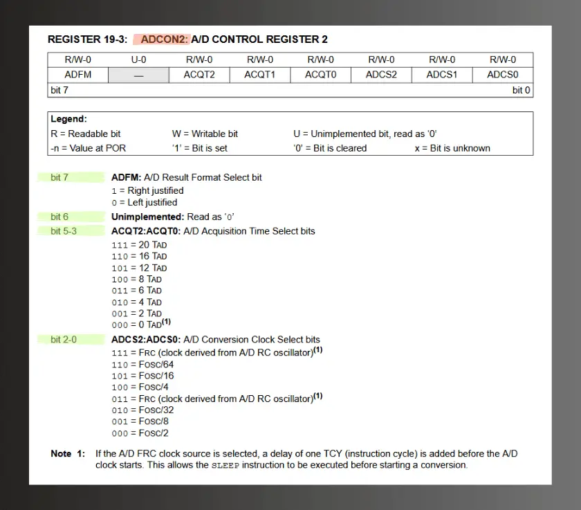
Let’s thoroughly walk through how one should set the bits for the ADCON2 control register for the purpose of setting up a PIC for using an analog input:
- Bit 7 is set to a logic ‘0’ to left-justify 8 bits in ADRESH, and 2 bits in ADRESL (bits b7 and b6) — or bit 7 is set to a logic ‘1’ to right-justify 2 bits in ADRESH (bits b1 and b0), and 8 bits in ADRESL, as seen the figure below. Later, we’ll left-justify this bit for this project, so we’ll set this bit to a logic ‘0’.
- Bit 6 is unimplemented, so its read as a logic ‘0’. We will set this bit to a logic ‘0’.
- Bits 5, 4, and 3, are used to select the TAD’s. The ‘T’ in TAD represents the period of the frequency of the timing waveform controlling the ADC conversion process. Recall from physics that the period of a waveform is given by the formula:
\begin{equation}
T = \frac{1}{f}
\end{equation}
T is the period (measured in seconds [sec]), and f is the frequency (measured in hertz [Hz])
- Bits 2, 1, and 0, are used to choose the RC oscillator as the timing source for the ADC or to divide the oscillator frequency by 2, 4, 8, 16, 32, or 64. The idea is to create a 2.4µs delay.
❓ Wait, what 🤔? Where did this idea to create a 2.4µs delay come from?!
🔔 Don’t worry! We’ll get into that and go step-by-step on how to setup bits 5 through 0 (b5 – b0), for the ADCON2 control register, next. Let’s first learn about the minimum required acquisition time (TACQ).
The Minimum Required Acquisition Time (TACQ)
When an analog-to-digital conversion begins, the PIC microcontroller internally connects the ADC to the selected analog input channel — the one receiving the external analog signal. In our case, we had only intended to use one analog input device for channel AN0, as mentioned in the ADCON1 discussion, above.
At that point, the voltage present on the input pin is sampled and temporarily stored by charging a capacitor inside the ADC’s sample-and-hold circuit. This charging process isn’t instantaneous; it takes a measurable amount of time for the capacitor to reach the input voltage level. That time is given by the formula for the time constant for an RC circuit:
\begin{equation}
\tau = RC
\end{equation}
τ is the time constant in seconds (s), R is resistance in ohms (Ω), and C is capacitance in farads (F)

Remember, we briefly talked about time-constants for Pin 1, or the MCLR pin on the PIC18F4525, in Part 2 of Programming a Super Simple LED Switch using a PIC microcontroller and the C programming language. We even went through making a calculation! It’s encouraged for you to go check that out, to learn more! Now, back to what we were talking about…
The duration depends on the capacitor’s size and the resistance at the input, both of which influence how quickly the voltage stabilizes. These characteristics vary between different PIC models. For the PIC18F4525 specifically, the sample-and-hold capacitor (CHOLD) is approximately 25 picofarads (see pg. 228, under section 19.1 of the datasheet), resulting in an estimated acquisition time of about 2.4 microseconds. You can see how the Minimum Required Acquisition Time (TACQ) is calculated from the equations shown on pg. 228, under section 19.1 of the datasheet:
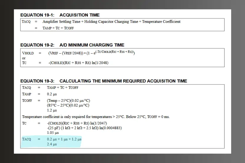
\begin{equation}
\boxed{T_{ACQ} = 2.4{\mu}{s}}
\end{equation}
So, what this minimum required acquisition time means is that we must get the PIC to wait 2.4µs before the ADC starts its conversion. If it doesn’t wait this amount of time, the result could be inaccurate. Luckily, Microchip (the manufacturer of the PIC) offers a couple of ways of creating this delay:
- We can manually create a delay routine that would need to be run every time before an ADC conversion starts. To do this, we’d perform the following:
- Set bits 5, 4, and 3, of the ADCON2 control register to a logic ‘0’. NOTE: we must be sure that we use this delay before the conversion begins and that it’s long enough. To start a conversion, we must set bit 1 of the ADCON2 control register to a logic ‘1’.
- We can automatically create a delay routine every time a conversion starts. To use this method, we need to know the period (T) of the frequency of the timing waveform controlling the ADC conversion process. Remember, we discussed how to do this earlier by using the equation T = 1/f. Microchip refers to this time period as “TAD” and provides several options for selecting its frequency. This flexibility exists because the PIC microcontrollers support a wide range of oscillator sources.
- Bits 2, 1, and 0, of the ADCON2 control register are used to choose the RC oscillator as the timing source for the ADC or to divide the oscillator frequency by 2, 4, 8, 16, 32, or 64. Again, the idea is to create a 2.4µs delay.
ADC Timing Process in a PIC Microcontroller
The steps below describe what happens internally when a PIC microcontroller performs an ADC (Analog-to-Digital Conversion):
- The ADC module is connected to the appropriate analog input pin.
- The voltage present at that input is sampled. This involves connecting the input to the PIC’s internal sample-and-hold circuit, which charges a capacitor to match the input voltage. The time required for the capacitor to charge is known as the acquisition time, and the microcontroller must wait long enough to ensure a full charge.
- The length of this wait time depends on the number of TAD periods you select as the programmer. You must ensure that the number of TAD periods is sufficient for the capacitor to fully charge. To do this, you must know how long each TAD period is.
- The TAD period is set using bits 0, 1, and 2 of the ADCON2 control register:
- ADCS0
- ADCS1
- ADCS2
- These bits allow you to choose the ADC’s clock frequency, which directly determines the TAD period.
- The TAD period corresponds to the clock cycle duration (“T”) of the frequency you select using the above bits in ADCON2.
- Therefore, the total acquisition time is determined by both:
- The number of TAD cycles you select, and
- the duration of each TAD cycle.
- One critical requirement is that the product of the number of TAD cycles and the TAD period must be equal to or greater than the required acquisition time. For example, if your TAD is 500ns, and the required acquisition time is 2.4µs, then the default minimum of 2 TAD periods only gives:
\begin{equation}
2\;x\;500\text{ns} = 1{\mu}{s}
\end{equation}
which is insufficient.
- Instead, selecting 6 TAD periods results in:
\begin{equation}
6\;x\;500\text{ns} = 3{\mu}{s}
\end{equation}
which satisfies the acquisition time requirement of 2.4µs for the PIC18F4525.
Example of Choosing an Acquisition Time
If we look back on our discussion on Setting Up the Oscillator (OSCCON), back in Part 3 of the Introduction to PIC Programming Using C: Programming a Super Simple LED, we had set up the configuration bits of the PIC to use its internal oscillator block as the primary oscillator source. We configured the bits in the OSCCON register to set the oscillator frequency at 8MHz.
Let’s say, for this example, that we’ll be setting the oscillator frequency (FOSC) at 8MHz, and that we choose a divide by 8 (FOSC/8), by making bits 2, 1, and 0 of the ADCON2 control register logic ‘0’, ‘0’, and ‘1’, respectively. This makes the frequency of the ADC operation 1MHz. This means that the analog-to-digital period (TAD) is 1 microsecond:
\begin{equation}
T_{AD} = \frac{1}{f}
\end{equation}
\begin{equation}
\frac{1}{1{\text{MHz}}} = \frac{1}{1,000,000[\frac{1}{s}]} = 1\;x\;10^{-6}[\text{s}]\;\equiv\;{1\text{E}^{-6}[\text{s}]} = \boxed{1{\mu}{s}}
\end{equation}
Remember: The period is a measure of time — in this case, a period of time in seconds.
To create the required acquisition time of 2.4µs (refer back to The Minimum Required Acquisition Time (TACQ)), we would need a 2.4 TAD time for the delay:
\begin{equation}
\frac{2.4{\mu}{s}}{1{\mu}{s}} = \frac{2.4\text{E}^{-6}}{1\text{E}^{-6}} = \boxed{2.4}
\end{equation}
If we look at the ADCON2 in the datasheet on pg. 225, of section 19.0 of the datasheet for the PIC18F4525 MCU, we see that the A/D Acquisition Time Select bits (bits 5-3) have no 2.4 TAD select option. There is a 2 TAD, but this is lower than we want. The next closest option is a 4 TAD, which is a greater value than 2.4µs, but the better option between the two.
The 2.4µs is the minimum, not the maximum time the PIC should allow for acquisition time. We should make the delay time as short as possible, but without making it too short, as the choice of 2 TAD would. So, a choice of 4 TAD is the next best choice and the shortest, compared to the others.
To write, in code, our selection of 4 TAD and the divide by 8, we’d set bits 5 to 0 (b5 to b0) of the ADCON2 control register as:
- bit 5-3: 010 = 4 TAD
- bit 2-0: 001 = FOSC/8
The following instruction in code will set the ADCON2 control register the way we have just described above:
\begin{equation}
\text{ADCON2} = 0b00010001
\end{equation}
\begin{equation}
\text{ADCON2} = 0x11;
\end{equation}
If you need to, you can visit our simple Hexadecimal-Binary-Decimal Unit Conversion calculator here, to see what the binary-to-hexadecimal conversion is. Just know that the binary value 0b00010001 is equivalent to the hexadecimal value 0x11.
Video: PIC Programming: Byte Lights With the ADC (Prototype Demo)
What’s Next?
Well, at this point, we’ve learned about the ADC of the PIC microcontroller and how to set it up for using an analog input. Now that we have the know-how of using the ADC — and referring back to what we learned on setting up a PIC for digital output, from our Super Simple LED Switch PIC Project Series — we’re now well equipped to create our prototype circuit and code in the following parts of this series!
In Part 2 of this series, we’ll begin to use what we’ve learned up to this point to create a prototype circuit that consists of an analog input from a variable voltage through a potentiometer to the PIC, and output a binary value to 8 LEDs that is analogous to the input signal coming into our circuit.
Later on, in Part 3 of this series, we’ll create the code for our prototype circuit, which will contain in it the values we’ve acquired here for the ADCON control registers. We’ll review the code, in detail, and then test our circuit to observe what we’ve created!
If, at any point you’ve felt confused about this material, or still feel you need another source of information on using a PIC microcontroller, I’ll share with you some recommendations and resources for learning the material of this subject matter, next.

Recommended Resources
First and foremost, before providing recommended resources for learning about PIC microcontrollers and programming them, it’s worth noting that, as with anything, it’s always best to get it straight from the horse’s mouth — or straight from the source, and that source is Microchip.
When needing resources for learning something, it’s always best to “get it straight from the horse’s mouth.”
Microchip Technology is the manufacturer of the PIC microcontrollers (and many other products), so going to them would be the obvious first recommendation to give. Their website and other social channels provide a wealth of information on PICs and other products they provide.
As for resources outside of Microchip’s scope, I recommend using other sources to really get an understanding of PIC microcontrollers — to be able to learn as much as you can.
Of course, the second obvious resource would have to be Motbots, where we’re currently active in providing learning material and projects for the PIC, as seen here, and are planning to add more material and projects on PIC microcontrollers in the near future. So, it’s encouraged for you to continue to check back in with us to see what’s new, from time-to-time.
Your best bet to stay informed on new material from us is by joining our Newsletter — we promise not to be spammy and to only send out notifications when something new hits the site.

As for other sources of material, I recommend getting Hubert Henry Ward’s book that I’ve referenced below. His book has offered me so much insight into the world of PIC microcontrollers, and his book really inspired me to create my own attempt at teaching how to use them. He’s even written an intermediate PIC programming book — that I’ve also got in my own personal library at home — that dives further into the world of PIC microcontrollers.
I also recommend checking out sites like DeepBlueEmbedded, or check out videos from creators on YouTube, like Microesque, and DeepBlueEmbedded — even smaller channels, like R Watson and zybytronic who have some great stuff and who are generous enough to share their knowledge with the world!
Another interesting channel is Darin Ulness’ GNL Project, where he has some introductory courses on the PIC microcontroller — though, neither are on the PIC18F4525, and he uses Assembly more than C, but he still offers valuable insights into how a PIC works and how to manipulate them with code. He does a great job in teaching about PICs.
Any information that you can find is very valuable, especially since it can be quite difficult to find anyone who does teach about them. Hopefully, in the near future, Motbots will provide PIC programming video content of its own, as well as more written content here on this site! You’ll have to stay tuned and join our Newsletter to stay informed!

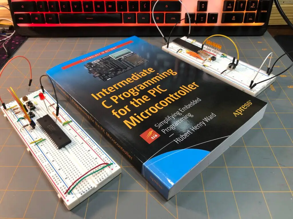
Book Reference
A lot of thanks needs to be given to Hubert Henry Ward and his book titled C Programming for the PIC Microcontroller. The knowledge that he’s shared in his book has not only helped me in my understanding of PIC programming in C, but I’m sure in many others as well.
Mr. Ward’s book starts you in the basics of what you need to know, gradually building your understanding of C programming, PIC microcontrollers, and the MPLABX software. His book will walk you through, step-by-step, during the learning process and on to applying what you’ve learned by performing easy-to-follow projects, often providing pictures within the pages.
In his book, you’ll participate in PIC projects like an LED traffic light, creating a volt meter and use an LCD screen to view voltage outputs. You’ll even delve deeper into some more useful code using the C programming language for the PIC microcontroller.
I highly encourage you to check out Mr. Ward’s book, C Programming for the PIC Microcontroller, so that you too can learn about PIC programming using C.

Conclusion
TAD timing is arguably one of the most confusing calculations you’ll encounter when working with PIC microcontrollers. Trust me, I’ve spent many, many hours reading and researching, not only what all of it is, but how to do it — and I’m still not confident in it!
So, don’t fret and don’t be intimidated by it. It’s only numbers, and you can do it. Just stick with it! I only hope that all my efforts here, to try and write in simple detail, that you’ve been able to at least understand a little bit of it. It’s quite a complex topic to write clearly about, I have to admit.
I hope that you’ve found the information here useful and really hope that this content has been helpful for you. I know that these basic steps of the process may seem intimidating, tedious, and boring to some, but as with all things new to learn, we must trudge through the tough stuff, so that we may gain a better understanding and experience on the subject matter.
If you’ve found this information useful, please leave us a comment below. We’d love to hear from you. Help spread the word about Motbots, so that we may help others with similar interests as you in electronics and robotics. Thanks for your time here! We’ll see you in Part 2! Remember to keep at it and stay motivated.