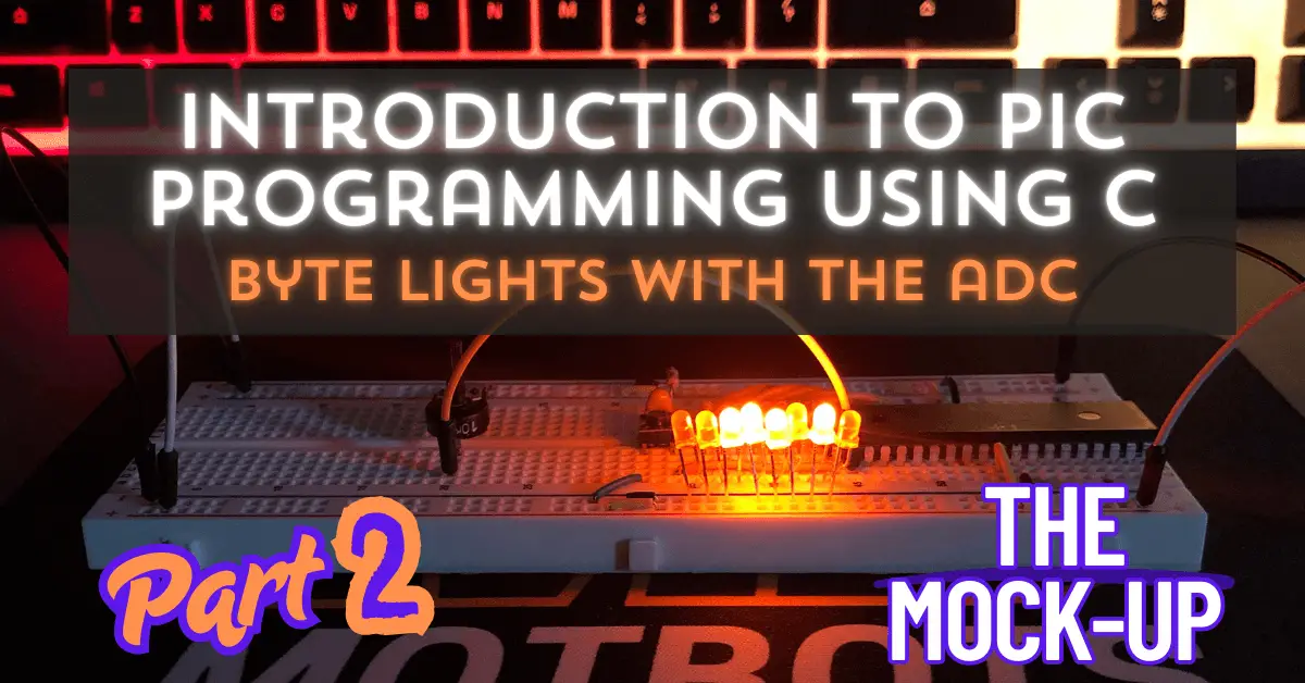
Introduction to PIC Programming Using C: Byte Lights With the ADC – Part 2: The Mock-Up
Introduction
Welcome back! In this series, we’re still continuing our goal to understand analog-to-digital conversion (ADC) of a PIC microcontroller, and how to program one to accept and convert an analog input. It is my personal goal to help guide you to do this in a way that I learned from a terrific book I purchased some time ago of which you can observe for yourself at the Book Reference at the bottom of this page.
The following is intended to be an enhancement to such pedagogical material that sometimes leaves more to be desired for the reader. It is the intention of the following to add more input to the learning material that is currently available, or currently unavailable, in the market today on learning how to program a PIC microcontroller using the C programming language.
Goal of This Project Series
The goal of this project series is to get us familiar with the ADC of a PIC microcontroller. We began this series with a discussion of what ADC means, and what the difference between analog and digital signals were.
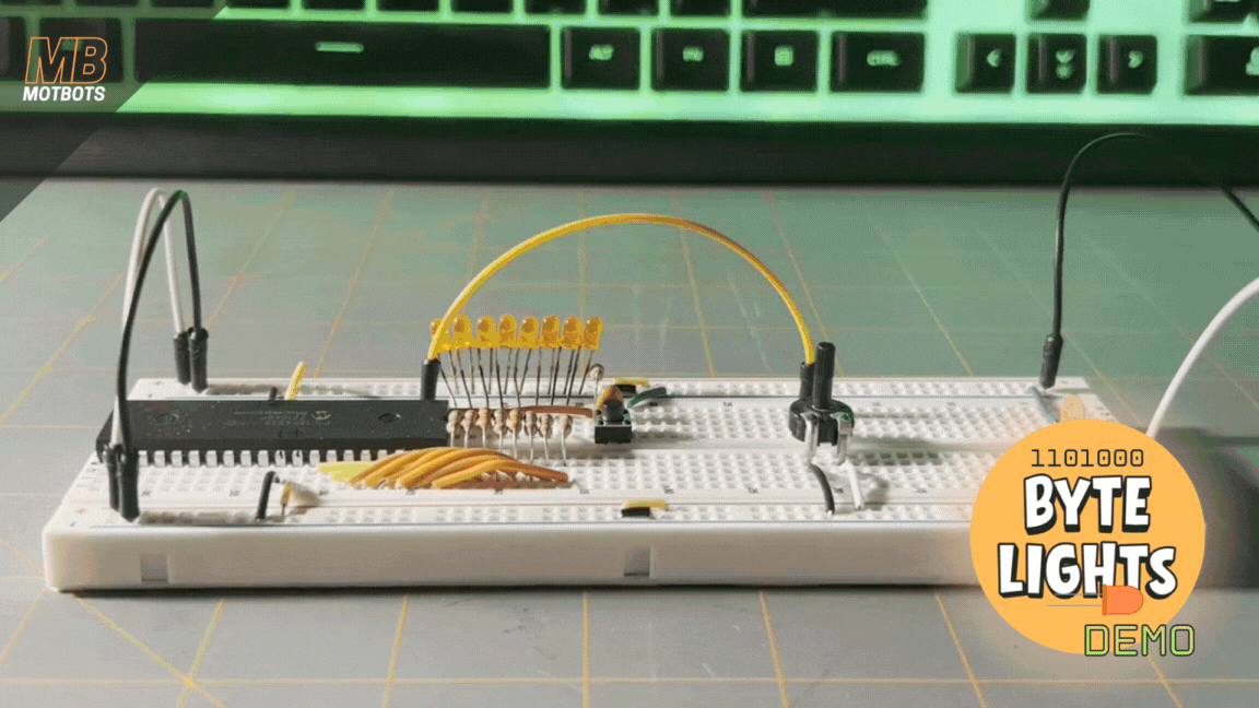
Next, we’ll actually take what we learned to visually see what’s happening when we take an analog input and convert it digitally by building a mock-up circuit consisting of 8 LEDs and a PIC microcontroller.
Later, for the final part of this series, we’ll thoroughly go over the code we’ll create to get a PIC microcontroller to do the conversion from analog to digital, so that we may see an output on our LEDs on our mock-up circuit showing us a converted signal to a visual binary format consisting of our LEDs either being ON or OFF.
The following is a quick reference to the sequence of this three part series on the Introduction to PIC Using C: Byte Lights With the ADC:
Three Part Series Sequence:
- Part 1: The ADC – This is when we learned about analog-to-digital conversion of a PIC microcontroller.
- Part 2: The Mock-Up – Here, we will build a mock-up circuit consisting of 8 LEDs that will provide a visual binary output of an analog input coming from a variable voltage signal through a potentiometer.
- Part 3: The Code – At this stage, we’ll walk through the code that sets up the PIC18F4525 microcontroller to read a single analog input and output 8 digital signals — lighting up LEDs to visually represent the variable input voltage.

This is Part 2: The Mock-Up
In Part 1 of this series, we already went over what ADC means, and what the difference between analog and digital signals were. We discussed common types of analog inputs, how to calculate the resolution of an ADC, and we thoroughly went over how we would set up a PIC18F4525 microcontroller and its registers to use analog inputs — like for what we want to do for this project!
As previously stated, in this part of the series our goal is to build a mock-up circuit on a breadboard consisting of 8 LEDs and a PIC18F4525 microcontroller that will provide a visual digital output of an analog input into the circuit coming from a variable voltage signal through a potentiometer.
In the final installment of this series, we’ll go over the code used to setup the PIC18F4525 microcontroller we’re using for this project to read an analog input, to then output eight digital signals to light up eight corresponding LEDs — doing so will visually represent the variable input voltage in byte format.
Recall that a byte is made up of 8 bits — each bit consisting of a binary signal of either ON or OFF, HIGH or LOW, 1 or 0.

Now that we know about the ADC, what analog and digital mean, and how to calculate the resolution of an ADC, let’s get to it with creating our mock-up circuit. Below is the list of parts and other items we’ll need to accomplish creating our byte lights circuit.
Parts List
| ITEM | QUANTITY |
| PIC18F4525 Microcontroller | 1 |
| 830-Point Solderless Breadboard | 1 |
| Breadboard Jumper Wires | Various Colors and Sizes |
| Male-to-Male Jumper Wires | Various Colors and Sizes |
| Orange LEDs — Diffused 5mm | 8 |
| 220Ω Resistors | 8 |
| 12Ω Resistor | 1 |
| 0.1µF Ceramic Capacitor | 1 |
| 10kΩ Breadboard Potentiometer w/ Knob | 1 |
| SPST-NO Momentary Tactile Push-Button Switch (two-terminal switch) | 1 |
Tools List
| ITEM | QUANTITY |
| 5V Power Supply | Benchtop Power Supply |
| PICkit 3 In-Circuit Debugger | 1 |
| Universal Programmer Seat Board Adapter | 1 |
| Microchips’s MPLAB Software Tools | MPLAB X v.6.15 |
A Quick Word on Power Supplies
As for the power supply for this project, I am using a Wanptek programmable benchtop power supply. Odd name, but a descent little power supply.
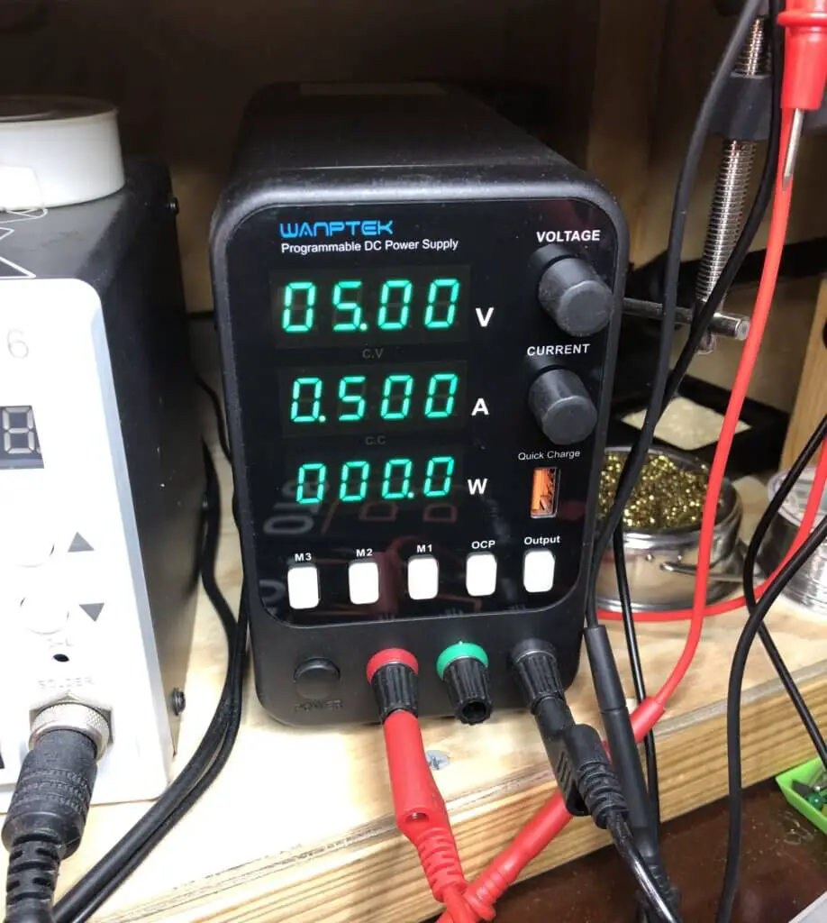
I purchased mine about a year or so ago now, and I’ve used it for many projects over that period of time. It’s a relatively cheap power supply (less than $100) and I have had no issues with mine to date. You can find many other cheap power supplies in the market that are even cheaper than mine and probably just as good.
Just make sure that you do your research and read the reviews of what people say about them, and try as best you can to stay away from the crummy ones. A descent power supply is a must have tool for any electronics hobbyist and will be used a lot for your projects.

Power supplies are easier to setup for power for your prototypes than batteries, and can be adjusted for just the right voltage you need than having to create a power supply circuit for each prototype circuit you make for all your projects.
A good benchtop power supply is a preferable source of power when working with PICs and prototyping their circuits. They’re more reliable, more stable, and time efficient when trying to quickly setup prototype and test circuits.
Trying to fiddle with unreliable power sources can often lead to damaging your PIC microcontrollers, which leads to money and time being wasted – don’t ask me how I know. Just know that I am very familiar with the smell of burning silicon and burning holes in my wallet.
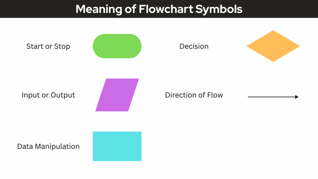
The Flowchart
To help us better understand what it is that we are trying to do, and what we want to accomplish for this project, let’s use the help of a flowchart. Below is a flowchart diagram for this project:
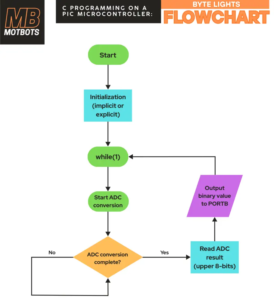
While the ADC is converting, the program repeatedly checks the conversion-complete condition and remains in this decision loop until the result is ready.
As you can see, a flowchart is a diagram that helps us to understand the flow of the code that we want to write. Being able to visualize how the code should work makes it much easier to think about how we should program the microcontroller.
It’s highly recommended to create a flowchart for when you are planning a coding project, especially one that will contain several actions in it and a microcontroller. Below is an explanation of what the symbols of a flowchart mean.
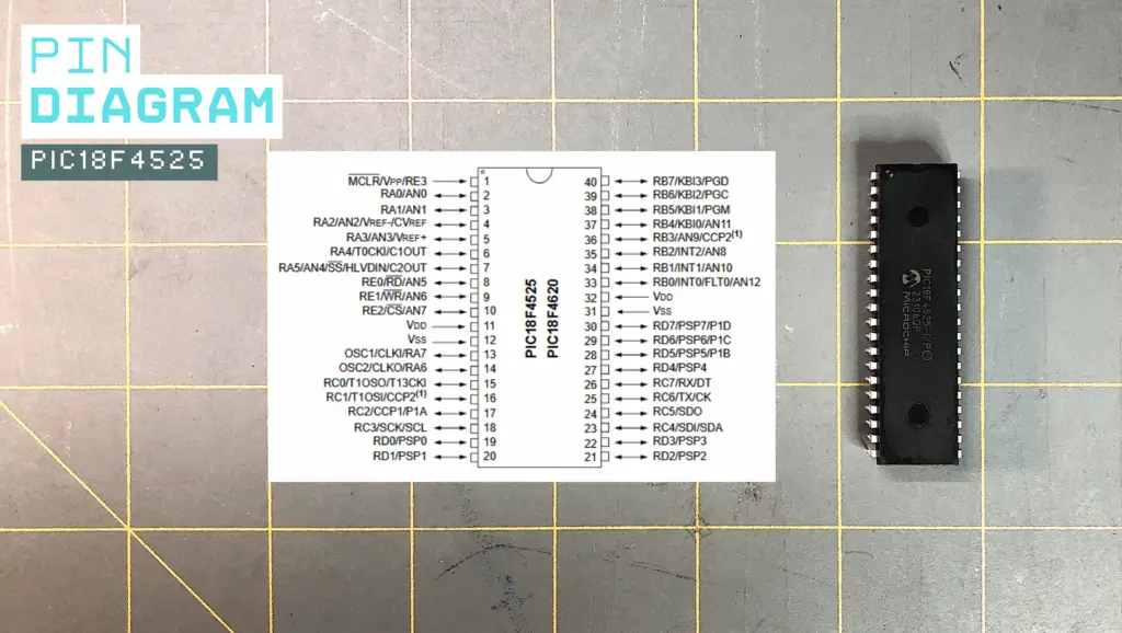
The PIC18F4525 Datasheet
It’s highly recommended that you download and observe the provided datasheet below for the PIC18F4525. We will be using the datasheet to thoroughly go over each pin we will use for this project. The datasheet is where we will find the information that we need to program the PIC.
Microchip PIC18F4525 Datasheet
Download the PIC18F4525 Datasheet
Schematic for the Mock-up Circuit
Now, let’s move on to the schematic of this project. A schematic shows a visual representation of the components we’ll use for our project and how each are to be connected in the circuit we’ll build.
The schematic, shown below, will help us understand how each component in this project will be connected to each other, to the power source, and to ground.

The schematic diagram above shows a representation of the PIC18F4525 microcontroller that we’re using for our byte lights project. If you look closely, you can see all the little numbered and labeled lines coming from the rectangular shape – that’s the microntroller! The little lines are a representation of the microcontroller’s pins.
Pin 1 (MCLR)
Starting at pin 1 — the MCLR pin — this pin will be used for our RESET switch (SW1). If we were to look at page 43 of the datasheet for the PIC18F4525 microcontroller, we’d see that this page explains as to what the Master Clear (MCLR) pin is for. The datasheet states that “the MCLR pin provides a method for triggering an external Reset of the device.”
What the MCLR pin does
On the PIC18F4525, the MCLR pin (pin 1) has two primary roles:
- External reset input (active-LOW)
- Optional programming voltage input (VPP) when using ICSP
When MCLR is held HIGH, the microcontroller runs normally. When MCLR is pulled LOW, the PIC immediately resets.
MCLR connections in the schematic
Looking at the schematic, the MCLR network consists of:
- A 10kΩ resistor (R9) — the pull-up resistor tied to +5V, and to capacitor (C1).
- A 0.1µF capacitor (C1), with its leads tied across the switch (SW1) or parallel with the switch.
- The switch (SW1) is a momentary push-button switch with one terminal tied to ground, and the other terminal tied to pin 1 (MCLR) of the PIC and to the +5V supply through resistor R9.
Normal operation (power applied)
When power is applied, resistor R9 pulls the MCLR pin of the PIC up to +5V (HIGH), during normal operation so the PIC runs. The PIC comes out of reset, and the program execution begins within the PIC. The pull-up ensures MCLR never “floats,” which would otherwise cause random resets.
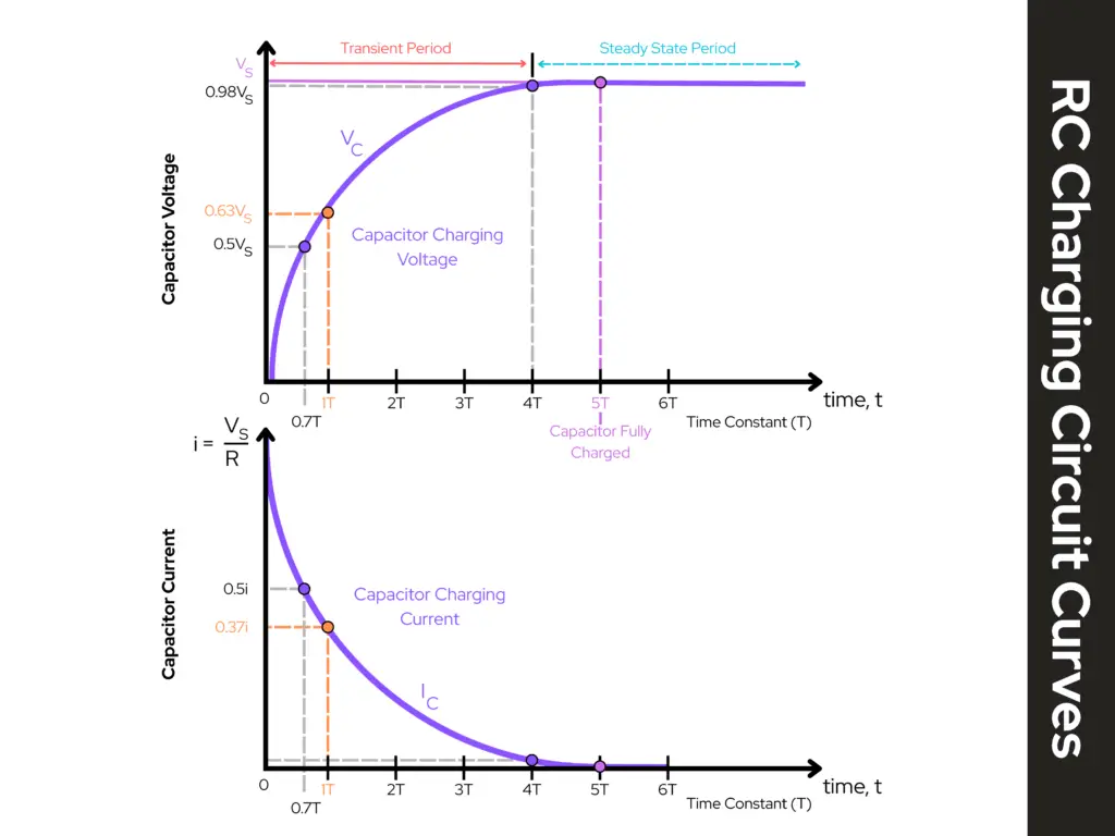
Power-on reset behavior (RC network)
The R9 and C1 combination creates a power-on reset delay when at power up, C1 is initially discharged and the MCLR pin (pin 1) rises slowly as C1 charges through R9. This short delay allows the power rail to stabilize and it prevents the PIC from starting in an undefined state. This improves reliability, especially on breadboards or long power leads.
Manual reset (push-button SW1)
When switch SW1 is pressed, the MCLR pin is directly shorted to ground (GND). The voltage on the MCLR pin drops to 0V, and the PIC immediately resets.
When switch SW1 is released, R9 pulls the MCLR pin back up to +5V, the capacitor (C1) recharges, and the PIC restarts cleanly from reset.
This is very useful for debugging, demonstrations, and for restarting code without power-cycling.
The reset “delay” (RC time constant)
One time-constant is written as:
\begin{equation}
\tau = R \times C
\end{equation}
So, if we plug-in the values for R9 and C1, we get:
\begin{equation}
\tau = 10kΩ \times 0.1µF
\end{equation}
\begin{equation}
\tau = 10,000Ω \times 0.0000001F
\end{equation}
\begin{equation}
\tau = 0.001\text{s}
\end{equation}
\begin{equation}
\boxed{\tau \approx 1\text{ms}}
\end{equation}
So MCLR rises toward +5V over a few milliseconds (rule of thumb: it’s “basically high” after approximately 5τ ≈ 5ms). That’s plenty for a clean start, and it’s right in line with common PIC practice.
Pin 2 (AN0)
If we look at pin 2 — the AN0 pin — on the PIC18F4525, we see that the center terminal (terminal 2) or wiper of a potentiometer (RV1) is connected to it. The other two terminals of the potentiometer are connected to the +5V supply (terminal 1) and to ground (terminal 3).
What pin 2 (AN0) is doing
On the PIC18F4525, pin AN0 is the primary analog input to the ADC — one of the most commonly used ADC channels on PIC18 devices. In our circuit, AN0 is intentionally used to introduce user-controlled analog input.
How the potentiometer works
The potentiometer is wired as a voltage divider, where one terminal (terminal 1) is connected to the +5V supply, another terminal (terminal 3) is connected to GND, and the center wiper is connected to pin AN0 of the PIC18F4525 microcontroller.
Turning the knob moves the wiper, producing a smooth voltage between 0V and +5V. This voltage is applied directly to AN0.
What the PIC does with AN0
Inside the PIC the ADC samples the voltage on AN0. The ADC then converts it into a 10-bit digital value:
- 0 V → 0
- 5 V → 1023
Where:
| Voltage Value | 10-bit Binary Equivalent Value | 10-bit Decimal Equivalent Value |
| 0V | 0000000000 | 0 |
| 5V | 1111111111 | 1023 |


The firmware uses that number to control program behavior (for example: LED timing, animation speed, brightness, or pattern selection). This creates a direct physical-to-digital interaction:
Turn the knob → voltage changes → ADC value changes → LEDs respond
Power Supply Pins
Looking at the schematic provided above for this project, it’s difficult to read the pin numbers for the PIC’s power and ground. So, let’s take a look at the Pin Diagram on page 4 of the datasheet so we can see the VDD and VSS pins.
Even though our schematic doesn’t quite show this, there are two VDD pins (pins 11 and 32) and two VSS pins (pins 12 and 31) on the PIC18F4525 microcontroller. We will connect both VDD pins to our positive power supply (+5V) and connect both VSS pins to our negative supply or ground (0V).
- VDD is used as the positive supply voltage
- VSS is used as the negative supply voltage
Looking at our schematic above, we see that we will connect both VDD pins together to the +5V supply. From this connection is a 0.1µF ceramic capacitor in parallel to it and ground. This capacitor acts to help stabilize the supply voltage feeding into the microcontroller, which is crucial for its operation.
Both VSS pins of the PIC18F4525 microcontroller will be tied to ground (GND), as can be seen in the schematic above for this project.
- Pins 11 and 32 of the PIC18F4525 microcontroller are its VDD pins.
- Pins 12 and 31 of the PIC18F4525 microcontroller are its VSS pins.
- Both VSS pins of the PIC will be tied to ground (GND).
- Both VDD pins of the PIC will be tied to the +5V power supply. A 0.1µF ceramic capacitor (C2) will be tied across this connection and ground to help stabilize this voltage for the PIC.
The decoupling capacitor (C2)
Capacitor C2, is a 0.1µF capacitor from the +5V rail to GND — tied across the incoming supply voltage to the circuit. This is a standard bypass/decoupling capacitor and it:
- supplies fast “instant” current to the PIC during switching
- reduces supply noise from LED switching / code execution
- helps keep the MCU stable (especially on a breadboard)
Right now C2 is shown across the rail, and later you’ll see that I placed this capacitor directly across the two jumper wires used to connect the power supply voltage to the breadboard. Ideally you would want to place it physically as close as possible to the PIC’s VDD/VSS pins and (even better) use one 0.1µF per VDD pin if the package has multiple supply pins. But, due to constraints on the breadboard (and probably carelessness on my part), I placed C2 as we see it currently.
Pins 33 through 40
Pins 33 through 40 on the PIC18F4525 correspond to PORTB (RB0–RB7).
Notice that pin 33 is considered to be RB0 for the PIC18F4525. This means that RB0 is bit 0 on PORTB. PORTB is one of the I/O ports of the PIC18F4525, that contains individual I/O pins for that port. Since the PIC18F4525 is an 8-bit PIC, it has up to 8 bits on each PORT ranging from bit 0 to bit 7.
- RB0 means bit 0 on PORTB
- RB1 means bit 1 on PORTB
- RB2 means bit 2 on PORTB
- RB3 means bit 3 on PORTB
- RB4 means bit 4 on PORTB
- RB5 means bit 5 on PORTB
- RB6 means bit 6 on PORTB
- RB7 means bit 7 on PORTB
In this project, these pins are configured as digital outputs and are used to drive a row of LEDs — the visual “Byte Lights” display.
How the LEDs are connected
Each PORTB pin connects to:
- A 220Ω current-limiting resistor
- Then to an LED
- Then to ground
This means the PIC is sourcing current when a PORTB pin is driven HIGH (~5V). The current flows from the pin to the resistor, to the LED, then to GND — the LED then turns ON.
When the pin is LOW (0V), there’s no current flow, and the LED turns OFF.
Each pin independently controls its own LED.
Why PORTB is ideal for this job
PORTB is especially well-suited for LED control because it’s a full 8-bit port, perfect for representing a “byte”. Also, each pin can be individually controlled, and it allows clean demonstrations of:
- binary counting
- bit patterns
- shifting and masking
- ADC-to-digital visual mapping
What the firmware does with PORTB
Later, in Part 3 of this series, we’ll go over the code thoroughly for this project. There, we’ll see that inside our code, PORTB will be set as an output (TRISB = 0x00). The program will write values directly to the PORTB register.
For example:
- PORTB = 0b00001111 will correspond to the lower four LEDs being ON and the upper four LEDs being OFF
- PORTB = 0b10101010 will correspond to alternating LEDs being OFF and ON
- ADC values can be scaled and displayed as changing bit patterns
This will create a direct, visible link between software and hardware.
Assembling the Prototype Circuit
A Helpful Tip (Marking the PIC)
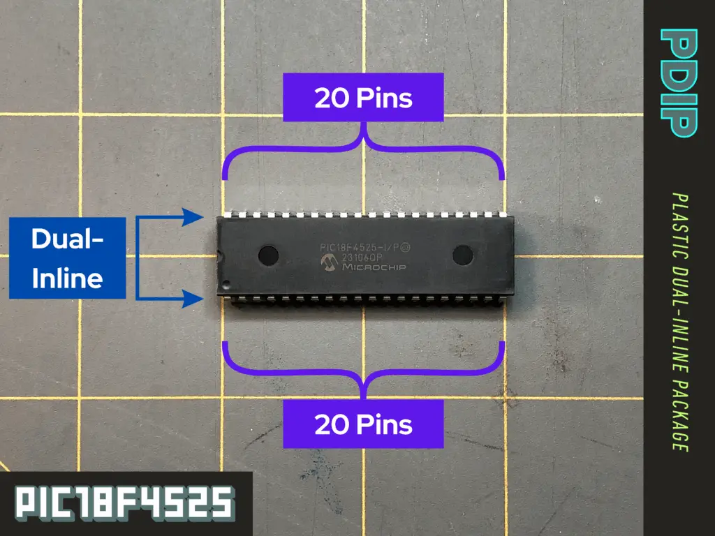
For this project, we’re using a dual-inline package (PDIP) for the PIC18F4525. The first “P” in PDIP stands for plastic. This means that the 40 pins that our PIC has is divided in two (dual) and are lined (in-line) on both the long sides of the PIC’s body (package).
40 pins is a lot, and it can become quite tedious to count them every time we are making connections to them. Also, we’ll need to remove and replace the PIC onto the breadboard when we need to write our code to it from the universal programmer seat adapter we’re using for the PICkit 3 programmer. So, to make things a bit easier, before we get to prototyping our circuit on a breadboard, I find it extremely helpful to make some marks directly onto the PIC’s body before I start making connections to its pins.
First, place your PIC down on a flat surface or into your breadboard with the pins facing down. Notice the small dimple in one of the PIC’s corners. Orient the PIC so that the small dimple it has for reference is in the top-left corner when facing you. This reference dimple is there to identify pin 1 of the PIC.
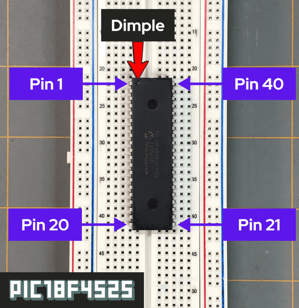
Pin 1 starts from the reference dimple in the top-left corner orientation, and the pin number sequence continues from there, the next pin being pin 2, then pin 3, and so on – down to pin 20, being the last pin on the left-hand side of the PIC.
The pin order continues on the right-hand side of the PIC, directly across from pin 20, where pin 21 begins on the bottom right-hand side of the PIC. From there, the pin number sequence continues, going on to pin 22, then to pin 23, and so on – working your way up the right-hand side of the PIC.
Now, grab yourself an ultra-fine tip permanent marker and take a look at the 40-Pin PDIP Pin Diagram for the PIC18F4525, found on page 2 of the datasheet. We see on the datasheet that pins 11 and 32 are both the VDD pins. These pins are both for the positive supply voltage for the PIC.
- Having the PIC with the top of its body facing up and the small dimple it has for reference for pin 1 in the top-left corner facing you, count to pin 11 down the left-hand side of the PIC. Make a “+” mark next to this pin directly on the body of the PIC.
- Now count up the right-hand side of the PIC to pin 32. Make a “+” mark next to this pin directly on the body of the PIC.
Looking at the Pin Diagram on the datasheet again, we see that pins 12 and 31 are both the VSS pins. These pins are both for the negative supply voltage for the PIC.
- Having the PIC with the top of its body facing up and the small dimple it has for reference for pin 1 in the top-left corner facing you, count to pin 12 down the left-hand side of the PIC. Make a “-” mark next to this pin directly on the body of the PIC.
- Now count up the right-hand side of the PIC to pin 31. Make a “-” mark next to this pin directly on the body of the PIC.
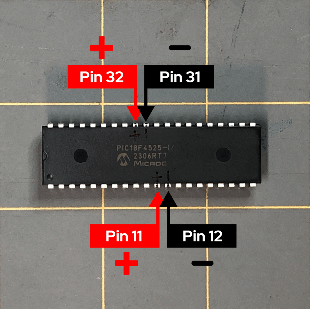
Having made these marks on the PIC’s body for the supply voltage will help in quickly placing your PIC correctly back onto the breadboard after removing it and lining up the connections you made on the breadboard. It’ll also help you quickly reference other pin numbers on the PIC from the datasheet, so that you don’t have to count so many pins all the time.
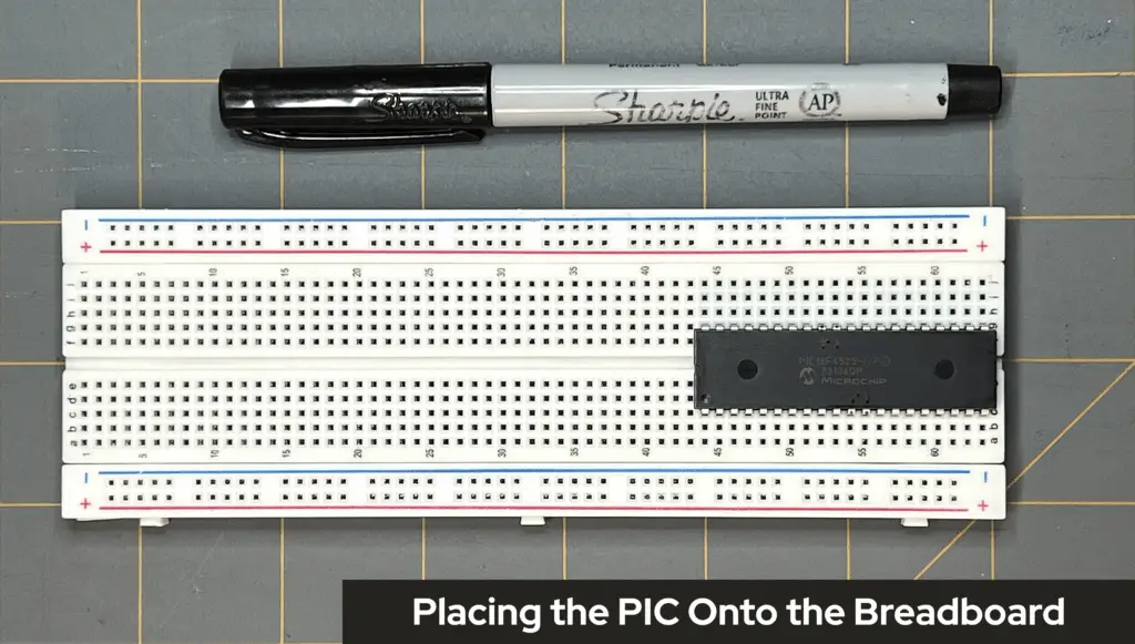
Placing the PIC Onto the Breadboard

Taking an 830-point solderless breadboard, I’ve aligned the PIC to be about center on the breadboard. I have placed pins 1 through 20 to be placed into points c44 to c64 of the breadboard, respectively. Pins 40 through 21 of the PIC have been placed into points g44 to g64 of the breadboard, respectively.
Making the Power Supply Connections
To make the proper connections for power for the PIC18F4525 and all other components that it’ll drive, I first started with where the 5V power supply will come into on the breadboard. Let’s go through this process, step-by-step:
- First, I’ve placed a 0.1µF ceramic capacitor (C2) in to points e4 and f4, of the breadboard.
- Second, I’ve taken a yellow jumper wire and have placed one lead of this jumper wire into point h4, inline with the capacitor’s lead. Next, I’ve placed the jumper wire’s opposite lead into a point on the right-side positive (+) vertical power rail of the breadboard.
- Third, I’ve taken a blue jumper wire and have placed one lead of this jumper wire into point d4, inline with the capacitor’s opposite-side lead. Next, I’ve placed the jumper wire’s opposite lead into a point on the left-side negative (-) vertical power rail of the breadboard.
- Fourth, to make the connections from my power supply later, to the breadboard, I added a longer white jumper wire to the right-side positive (+) power supply rail we’ve established, and I’ve added a longer black jumper wire to the left-side negative (-) power supply rail we’ve established.
- Fifth, I’ve taken a longer white jumper wire to connect both positive (+) vertical power rails of either side of the breadboard. I’ve also taken a longer black jumper wire to connect both negative (-) vertical power rails of either side of the breadboard.
- To continue these paths along the entire length of each power rail (for both positive and negative), I’ve added smaller yellow jumper wires to the middle of the positive power rails on both sides of the breadboard, as well as smaller black jumper wires to the middle of the negative power rails on both sides of the breadboard — completing the connection throughout the entire positive and negative rails along either side of the breadboard.
- Finally, to make the connections of the 5V power supply and ground directly to the PIC itself, I used the help of the marks that were made previously on the PIC with a permanent marker to help me to quickly determine which pins were the VDD (positive supply) and VSS (negative supply) pins. I took two yellow jumper wires and made the connections from those labeled positive (+) marks for the VDD pins (pins 11 and 32) to their neighboring positive (+) power rail supply. I took two black jumper wires and made the connections from those labeled negative (-) marks for the VSS pins (pins 12 and 31) to their neighboring negative (-) power rail supply.


Now, that we have the power supply set up to the breadboard and to the PIC, let’s move on to setup the MCLR connection, which will be for our Reset button for the PIC.
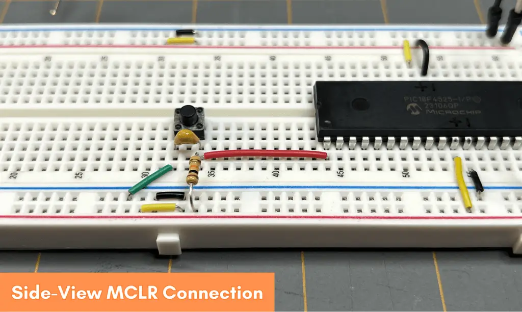
MCLR Connection to Pin 1
To make the MCLR connection for the Reset button for the PIC18F4525, I took a red jumper wire and placed one of its leads inline with pin 1 of the PIC MCU at point b44, on the breadboard. I placed the other end of the jumper wire at point b34. I then placed the 10kΩ resistor (R9) and one of its leads inline with the red jumper wire lead at point a34 on the breadboard. I placed the opposite lead of the resistor into one of the neighboring positive (+) power supply points of the breadboard.
Next, I made my branch connection from the lead of R9, at point a34, where it goes to the lead of the 0.1µF capacitor (C1). I placed a lead of C1 at point c34, and its other lead at point c32 on the breadboard. To place the push-button switch in parallel to the capacitor, I placed its leads at points e34 and e32. To complete this connection to ground, I took a small green jumper wire and placed one end into point a32 — inline with the leads of C1 and the push-button switch (SW1) — to a point in the neighboring negative (-) power rail supply.


Connecting the Potentiometer to Pin 2
To connect the potentionmeter (RV1) to pin 2 of the PIC MCU, I first made a connection from pin 2 using a long yellow jumper wire to the wiper of RV1. I took one end of the yellow jumper wire and placed it at point b45, inline with pin 2, and then placed the other end of the yellow jumper wire at point b20 on the breadboard. From there, I placed the wiper of RV1 at point e20 — inline with the yellow jumper wire at point b20 — and its other two leads at points g19 and g21, on the breadboard.
Next, I took a small white jumper wire and placed one of its ends at point h19 — inline with the lead of RV1 at point g19 — and placed the other end of the jumper wire into one of the neighboring positive (+) power supply points of the breadboard.
I then took a small black jumper wire and placed one of its ends at point h21 — inline with the lead of RV1 at point g21 — and placed the other end of the jumper wire into one of the neighboring negative (-) power supply points of the breadboard.


Connecting the LEDs to PINS 33 thru 40
At this point, all that is needed to complete the mock-up of the byte lights circuit is to make the connections for all eight LEDs (D1 to D8) and their current limiting resistors (R1 to R8) to pins 33 to 40 of the PIC18F4525 MCU. Let’s go through this, one LED and resistor at a time, in the following sequence:
- D1 and R1: I took a yellow jumper wire and placed one end of it at point h51 on the breadboard — inline with pin 33 of the PIC — and the other end of the jumper wire at point h43. Next, I took a 220Ω resistor (R1) and placed one of its leads at point g43 — inline with the yellow jumper wire — and its other lead at point e43 on the breadboard. Then, I took an LED (D1) and placed its anode at point a43 — inline with the lead of R1 — and its cathode into one of the neighboring negative (-) power supply points of the breadboard.
- D2 and R2: I took a yellow jumper wire and placed one end of it at point i50 on the breadboard — inline with pin 34 of the PIC — and the other end of the jumper wire at point i42. Next, I took a 220Ω resistor (R2) and placed one of its leads at point g42 — inline with the yellow jumper wire — and its other lead at point e42 on the breadboard. Then, I took an LED (D2) and placed its anode at point a42 — inline with the lead of R2 — and its cathode into one of the neighboring negative (-) power supply points of the breadboard.
- D3 and R3: I took an orange jumper wire and placed one end of it at point j49 on the breadboard — inline with pin 35 of the PIC — and the other end of the jumper wire at point i41. Next, I took a 220Ω resistor (R3) and placed one of its leads at point g41 — inline with the orange jumper wire — and its other lead at point e41 on the breadboard. Then, I took an LED (D3) and placed its anode at point a41 — inline with the lead of R3 — and its cathode into one of the neighboring negative (-) power supply points of the breadboard.
- D4 and R4: I took an orange jumper wire and placed one end of it at point j48 on the breadboard — inline with pin 36 of the PIC — and the other end of the jumper wire at point i40. Next, I took a 220Ω resistor (R4) and placed one of its leads at point g40 — inline with the orange jumper wire — and its other lead at point e40 on the breadboard. Then, I took an LED (D4) and placed its anode at point a40 — inline with the lead of R4 — and its cathode into one of the neighboring negative (-) power supply points of the breadboard.
- D5 and R5: I took an orange jumper wire and placed one end of it at point j47 on the breadboard — inline with pin 37 of the PIC — and the other end of the jumper wire at point i39. Next, I took a 220Ω resistor (R5) and placed one of its leads at point g39 — inline with the orange jumper wire — and its other lead at point e39 on the breadboard. Then, I took an LED (D5) and placed its anode at point a39 — inline with the lead of R5 — and its cathode into one of the neighboring negative (-) power supply points of the breadboard.
- D6 and R6: I took an orange jumper wire and placed one end of it at point j46 on the breadboard — inline with pin 38 of the PIC — and the other end of the jumper wire at point i38. Next, I took a 220Ω resistor (R6) and placed one of its leads at point g38 — inline with the orange jumper wire — and its other lead at point e38 on the breadboard. Then, I took an LED (D6) and placed its anode at point a38 — inline with the lead of R6 — and its cathode into one of the neighboring negative (-) power supply points of the breadboard.
- D7 and R7: I took an orange jumper wire and placed one end of it at point j45 on the breadboard — inline with pin 39 of the PIC — and the other end of the jumper wire at point i37. Next, I took a 220Ω resistor (R7) and placed one of its leads at point g37 — inline with the orange jumper wire — and its other lead at point e37 on the breadboard. Then, I took an LED (D7) and placed its anode at point a37 — inline with the lead of R7 — and its cathode into one of the neighboring negative (-) power supply points of the breadboard.
- D8 and R8: I took an orange jumper wire and placed one end of it at point j44 on the breadboard — inline with pin 40 of the PIC — and the other end of the jumper wire at point i36. Next, I took a 220Ω resistor (R8) and placed one of its leads at point g38 — inline with the orange jumper wire — and its other lead at point e38 on the breadboard. Then, I took an LED (D8) and placed its anode at point a38 — inline with the lead of R8 — and its cathode into one of the neighboring negative (-) power supply points of the breadboard.


Now that we’ve made the connections to the pins of the PIC on our breadboard mock-up circuit, we’re ready to begin the process of creating the code for the PIC. We’ll do that and learn more in Part 3 of this Introduction to PIC Programming Using C: Byte Lights With the ADC project!
Video Build of the Byte Lights Project
VIDEO COMING SOON!

What’s Next?
We’re getting really close to the end of this project, and we’ve learned a lot along the way. It’s all coming together now! There’s just one final — and crucial — part left: the code that will run on our PIC microcontroller. That’s exactly what we’ll explore in Part 3 of Byte Lights With the ADC.
I hope you’ve found this information useful and that it’s helped you along your learning journey. If it has, feel free to leave a comment below—we’d love to hear your thoughts. And if you enjoyed this content, help spread the word about Motbots so we can reach and support others who share your interest in electronics and robotics.
We hope to proceed here, at Motbots, in developing more projects and ideas for you in the near future. Until then, keep at it and stay motivated!
Book Reference
A lot of thanks needs to be given to Hubert Henry Ward and his book titled C Programming for the PIC Microcontroller. The knowledge that he’s shared in his book has not only helped me in my understanding of PIC programming in C, but I’m sure in many others as well.
Mr. Ward’s book starts you in the basics of what you need to know, gradually building your understanding of C programming, PIC microcontrollers, and the MPLABX software. His book will walk you through, step-by-step, during the learning process and on to applying what you’ve learned by performing easy-to-follow projects, often providing pictures within the pages.
In his book, you’ll participate in PIC projects like an LED traffic light, creating a volt meter and use an LCD screen to view voltage outputs. You’ll even delve deeper into some more useful code using the C programming language for the PIC microcontroller.
I highly encourage you to check out Mr. Ward’s book, C Programming for the PIC Microcontroller, so that you too can learn about PIC programming using C.