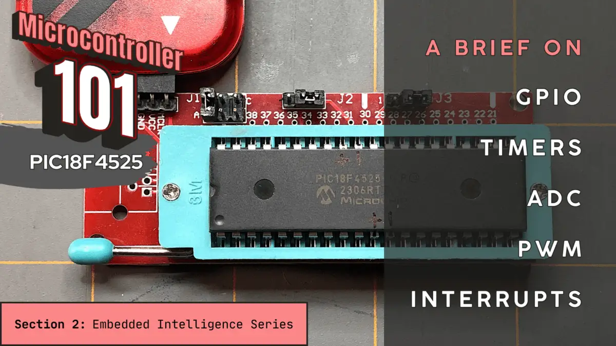
Microcontroller 101: A Brief on GPIO, Timers, ADC, PWM, and Interrupts (PIC18F4525)
Introduction
In Part 5, of the Circuit Component Super Series, we introduced microcontrollers as the control layer — the decision-making core that transforms simple circuits into intelligent systems. Now it’s time to go deeper and understand how it works internally.
This article breaks down the fundamental building blocks you’ll encounter in nearly every microcontroller project:
- GPIO basics
- Timers and delays
- ADC (Analog-to-Digital Conversion)
- PWM (Pulse-Width Modulation)
- Interrupts
- Debouncing buttons
These aren’t advanced features, they’re the foundation of embedded systems — master these, and you can control almost anything.
Welcome to the Embedded Intelligence Series
Welcome to the Embedded Intelligence Series, a sub-series to Part 5, of the Circuit Component Super Series, titled “From Circuits to Smart Systems: Introducing Microcontrollers”.
This is the second section of the Embedded Intelligence Series — Microcontroller 101: GPIO, Timers, ADC, PWM, and Interrupts (PIC18F4525), where the title and the introduction above explains what it’s about.
The Embedded Intelligence Series will provide you a continuation on the microcontroller — further advancing your, knowledge, know-how, and skill on the microcontroller. This series and its sections will be structured as follows:
- Section 1: Microcontroller 101 (ATmega328P)
- Section 2: Microcontroller 101 (PIC18F4525) (⬅️ YOU ARE HERE)
- Section 3: Real-World Interfacing
- Section 4: Smart Behavior
- Section 5: Next Steps
- Section 6: Arduino LED Blinker (Project)
- Section 7: PIC Temperature-Controlled Fan (Project)
This series expands on the foundational concepts of microcontrollers and takes you deeper into how they function internally — and more importantly, how to configure and program them to bring your designs to life.
So, let’s get started with some more basics — GPIO basics, next.
GPIO Basics (General Purpose Input/Output)
GPIO pins are the most basic way a microcontroller connects to the outside world. They’re versatile digital signal pins that can be configured to receive input signals or send output signals, depending on what your needs are:
- Input – Reads voltage level
- Output – Drives voltage level
The input mode is used to detect button presses, read digital sensors, or even monitor switches. Pins must not be left floating though, so that’s why we use pull-up resistors or pull-down resistors to help alleviate this.
The output mode is used to drive LEDs, trigger transistors, or enable motor drivers, for example. It’s important to note though, that GPIO pins cannot drive high current loads directly. External components, like MOSFETs are still required.
Again, GPIO (General Purpose Input/Output) pins are the primary way a microcontroller interacts with the outside world, but not all GPIO implementations are the same.
GPIO Pins: Microchip PIC18F4525
Total GPIO Pins
The PIC18F4525 (40-pin DIP version) provides 36 I/O pins (depending on configuration), organized into ports:
- PORTA
- PORTB
- PORTC
- PORTD
- PORTE
This is significantly more raw I/O than the Arduino Uno.
Voltage Levels
The voltage levels of the PIC18F4525 are as follows:
- Typical Operating Voltage: 5V
- Logic HIGH ≈ VDD
- Logic LOW ≈ 0V
⚠️ Most pins are not 5V tolerant above VDD. If running at 5V, do not exceed that level.
Current Capabilities
The PIC18F4525’s current capabilities are:
- Per Pin: ~25mA typical limit (check datasheet)
- Total Device Limit: Usually ~200mA across all pins
Like the Arduino, high-current loads on a PIC18F4525 require external drivers.
Pin Direction Control (Register-Level)
Unlike Arduino’s abstraction, a PIC requires direct register configuration. Each port has:
- TRISx: Controls direction
- 1 = Input
- 0 = Output
- LATx: Output latch register
- PORTx: Read input register
For example:
TRISBbits.TRISB0 = 0;   // Set RB0 as output
LATBbits.LATB0 = 1; // Drive RB0 HIGHThis provides more hardware awareness, more precision, and more responsibility when working with a PIC.
Analog vs Digital Configuration
PIC pins default to analog in many cases, which means you must configure the ADCON1/ANSEL registers (depending on variant). If not disabled, analog mode prevents digital functionality.
This is something that the Arduino hides automatically, but a PIC requires you to understand it.
Let’s take a look at the key differences between the Arduino Uno — the microcontroller we studied in the previous section of this sub-series (Section 1) — and the PIC18F4525, in the table below.
Key Structural Differences (Arduino Uno vs PIC18F4525)
| Feature | Arduino Uno (ATmega328P) | PIC18F4525 |
| Ease of Use | Very beginner-friendly. High-level functions like pinMode(), digitalWrite(), and analogRead() simplify hardware control. | More hardware-focused. Requires direct register configuration and understanding of peripherals. |
| GPIO Count | 14 digital I/O pins (6 with PWM), plus 6 analog inputs (shared with digital pins). | Up to 36 I/O pins (depending on configuration). More flexible pin usage but requires manual setup. |
| Configuration | Most peripherals configured automatically by Arduino core libraries. | All peripherals configured manually (ADCONx, TRISx, CCPx, TMRx, etc.). Full control, but more responsibility. |
| Default Pin Mode | Pins default to INPUT at reset. Arduino functions handle mode changes easily. | Many pins default to analog inputs at reset (depending on config bits). Must explicitly configure digital vs analog. |
| Learning Depth | Great for rapid prototyping and learning programming concepts. Hardware details are abstracted. | Excellent for learning how microcontrollers truly operate at the register level. Encourages deeper embedded understanding. |
Timers and Delays
Microcontrollers execute millions of instructions per second, but embedded systems must interact with real-world time, such as:
- Blink an LED every second
- Generate PWM signals
- Measure pulse width
- Schedule events
- Debounce buttons
- Run multitasking loops
Timers convert clock cycles into usable time. Without timers, everything would either block or be wildly inaccurate.
Let’s next go over the timers and delays for the Microchip PIC18F4525.
PIC18F4525 Timers and Delays
The PIC18F4525 includes four hardware timers:
| Timer | Resolution | Notes |
| Timer0 | 8/16-bit | Flexible |
| Timer1 | 16-bit | Precise |
| Timer2 | 8-bit | Often for PWM |
| Timer3 | 16-bit | Optional use |
Compared to the Arduino Uno, a PIC gives more granular control, but requires more setup.
System Clock
The PIC18F4525 can run up to 40 MHz (with PLL) — often 8 – 20 MHz typically. PLL (Phase-Locked Loop) is a hardware circuit used to multiply a clock frequency.
The instruction cycle frequency is:
\begin{equation}
\frac{F_{OSC}}{4}
\end{equation}
Where FOSC is the oscillator frequency. So, if the PIC were running at 20 MHz, then the instruction clock (instruction cycle frequency) would run at:
\begin{equation}
\frac{F_{OSC}}{4} = \frac{20\text{ MHz}}{4} = 5\text{ MHz instruction clock}
\end{equation}
This matters when calculating timing.
Timer0 Example
The Timer0 module can operate as 8-bit or 16-bit, with or without a prescaler.
The prescaler options are from 1:2 up to 1:256. For example, if our instruction clock were 5 MHz (above), and the prescaler was 256, then each timer tick would be:
\begin{equation}
\frac{5\text{ MHz}}{256} = \frac{\text{5,000,000 Hz}}{256} \approx \text{19,531 Hz}
\end{equation}
\begin{equation}
\frac{1}{\text{19,531 Hz}} = \frac{1}{\text{19,531 [}\frac{1}{\text{s}}\text{]}} = 0.0000512\text{ s} \approx 51\mu\text{s}
\end{equation}
So, with the PIC running at 20 MHz, and its instruction clock being 5 MHz, with the Timer0 module having a prescaler of 256, then each timer tick would be approximately 51µs (microseconds).
A tick = one time the timer register increases by 1.
Timer Registers
The example configuration for timer registers for a PIC are the:
- T0CON (Timer0 control register)
- TMR0L / TMR0H (Timer value registers)
- INTCON (interrupt control)
Unlike the Arduino, nothing is abstracted on the PIC. You configure every bit manually.
Timer2 (PWM Timing Base)
The Timer2 module often serves as the time base for PWM modules. It uses PR2 (period register), prescaler, and postscaler.
This separation of timing hardware is powerful for motor control and real-time control systems.
Timer Interrupt Example
A conceptual example of a timer interrupt for a PIC is as follows:
void __interrupt() ISR(void) {
    if (INTCONbits.TMR0IF) {
        LATBbits.LATB0 ^= 1;
        INTCONbits.TMR0IF = 0;
    }
}The PIC requires enabling global interrupts, enabling peripheral interrupts, and clearing interrupt flags manually. This is more work, but this gives you more control.
Let’s take a look at the key differences between the Arduino Uno — the microcontroller we studied in the previous section of this sub-series (Section 1) — and the PIC18F4525, in the table below.
Key Differences Between the Arduino Uno and PIC18F4525 (Timers and Delays)
| Feature | Arduino Uno (ATmega328P) | PIC18F4525 |
| Abstraction | High-level abstraction. Functions like delay(), millis(), and micros() hide timer hardware details. | Low-level control. Timers must be configured manually using registers (T0CON, T1CON, T2CON, etc.). |
| Ease of Use | Very simple for beginners. Delays and timing functions work immediately with minimal setup. | Requires understanding prescalers, instruction clock, preload values, and interrupt flags. More setup required. |
| Timer Setup | Timer0 is preconfigured by the Arduino core to support millis() and delay(). Users rarely touch timer registers directly. | Timers must be explicitly configured (mode, prescaler, clock source, preload value, interrupt enable). Nothing runs automatically. |
| millis() Available | Yes. Built-in function that returns milliseconds since program start. | No built-in function. Must create your own periodic timer interrupt and counter variable. |
| Instruction Clock | Runs at 16 MHz on standard Uno. Instruction clock = 16 MHz (single-cycle core). | With 8 MHz internal oscillator, instruction clock = FOSC/4 → 2 MHz. Timer calculations must account for this divide-by-4 architecture. |
An Arduino is convenient to use, but using a PIC teaches you timing math deeply.

ADC (Analog-to-Digital Conversion)
An ADC (Analog-to-Digital Converter) converts a continuously varying voltage into a digital number that firmware can process.
Microcontrollers cannot measure “temperature” or “light”, they measure voltage. The ADC translates that voltage into a binary value.
PIC18F4525 ADC
Resolution
The PIC18F4525 ADC, like the ATmega328P ADC, has a 10-bit resolution. Its output range is also between 0 and 1023, inclusive — the same numeric resolution as the Arduino.
Analog Channels
The PIC18F4525 supports up to 13 analog channels (depending on configuration). These are multiplexed into a single ADC module. You select the channel using the ADCON0 register.
Reference Voltage Options
The ADC does not measure voltage directly. It compares the input voltage to a known reference voltage.
Think of it like a ruler. If your ruler is 5 inches ling, you divide that into 1024 steps (10-bit ADC).
If your ruler is 2.5 inches long, you divide that length into 1024 steps. The number of steps stays the same — the scale changes.
The PIC18F4525 allows you to configure:
- Vref+ (Positive refernece)
- Vref- (Negative reference)
These define the measurement range. The most common configuration (default mode) being:
- Vref+ = VDD (typically 5V)
- Vref− = VSS (0V)
This means that:
- 0V: ADC = 0
- 5V: ADC = 1023
The resolution per step then, is:
\begin{equation}
\frac{5\text{V}}{1024} \approx 4.88\text{ mV per step}
\end{equation}
This is simple and requires no extra wiring, but it ties your ADC accuracy to your power supply stability. If VDD fluctuates, then your ADC scale shifts.
The PIC18F4525 provides a dedicated Vref+ input pin. You can connect a precise external voltage reference here. For example:
- Vref+ = 2.500V precision reference
- Vref- = 0V
Now:
\begin{equation}
0\text{V} \equiv 0
\end{equation}
\begin{equation}
2.5\text{V} \equiv 1023
\end{equation}
The resolution becomes:
\begin{equation}
\frac{2.5\text{V}}{1024} \approx 2.44\text{ mV per step}
\end{equation}
That is twice the resolution compared to 5V reference.
You can also set both reference limits externally. For example:
- Vref+ = 4.0V
- Vref− = 1.0V
Now the ADC measures only the range:
\begin{equation}
1.0\text{V} \equiv 0
\end{equation}
\begin{equation}
4\text{V} \equiv 1023
\end{equation}
This is powerful as your sensor operates in a limited voltage range or you want to maximize resolution within that range. The resolution now is:
\begin{equation}
\frac{(4.0\text{V} – 1.0\text{V})}{1024} \approx 2.93\text{ mV per step}
\end{equation}
You effectively “zoom in” on a specific voltage band.
ADC Clock Source
ADC conversion requires a clock derived from FOSC (oscillator frequency) divided by the selectable prescaler. Those options include:
- FOSC / 2
- FOSC / 8
- FOSC / 32
- Internal RC clock
Correct selection is critical. Too fast and you get an inaccurate conversion. Too slow and you get an unnecessary delay.
Acquisition Time
The acquisition time is very important. The PIC requires a minimum acquisition time before conversion. The reason is because the ADC uses an internal sample-and-hold capacitor.
This capacitor must charge to the input voltage level before conversion. If the acquisition time is too short, then the readings are inaccurate, especially with high source impedance sensors. This is something Arduino hides automatically.
Conversion Time
The ADC conversion time is the total time required for the microcontroller to convert an analog voltage into a digital voltage. For the PIC18F4525, the total ADC time consists of two phases:
- Acquisition Time (Tacq)
- Conversion Time (Tconv)
The total ADC time is:
\begin{equation}
T_{total}\;=\;T_{acq}\;+\;T_{conv}
\end{equation}
Many people only think about conversion time — but acquisition time is just as important.
Before conversion begins, the ADC must connect the selected analog channel, charge an internal sample-and-hold capacitor, and allow the capacitor voltage to settle.
The PIC ADC includes a small internal capacitor (~120pF typically). If your sensor has a high source impedance (like a thermistor divider, similar to the one in the 555 Temperature-Controlled Fan Controller), the capacitor charges more slowly. If you don’t wait long enough, then:
- The voltage doesn’t fully settle
- The reading is lower than actual
- Results become inconsistent
That’s why PIC requires a minimum acquisition time before starting conversion — a typical acquisition time of approximately 2-5µs (depending on source impedence).
Once acquisition is complete, the ADC performs the actual conversion. The PIC18F4525 uses a successive approximation ADC. The conversion requires 12 TAD Cycles, where TAD is the ADC clock period.
TAD is derived from:
\begin{equation}
\frac{F_{OSC}}{\text{prescaler}}
\end{equation}
For example, if the FOSC is 20MHz, and the ADC clock is FOSC/32, then:
\begin{equation}
\frac{F_{OSC}}{32} = \frac{20\text{ MHz}}{32} = 625\text{ kHz}
\end{equation}
So, the TAD becomes:
\begin{equation}
\text{TAD} = \frac{1}{625\text{ kHz}} = \frac{1}{\text{625,000 Hz}} \approx 1.6\mu\text{s}
\end{equation}
Now, if we calculate the conversion time:
\begin{equation}
12\;\text{x}\;\text{TAD}\:=\:12\;\text{x}\;1.6\mu\text{s}\:\approx\:19.2\mu\text{s}
\end{equation}
That’s the pure conversion phase.
Now, we add the acquisition time. Let’s assume:
\begin{equation}
T_{acq}\:=\:5\mu\text{s}
\end{equation}
Then, the total ADC time becomes:
\begin{equation}
T_{total}\:=\:5\mu\text{s}\:+\:19.2\mu\text{s}\:\approx\:24.2\mu\text{s}
\end{equation}
That means that the maximum theoretical sampling rate is:
\begin{equation}
\frac{1}{24.2\mu\text{s}}\:\approx\:41\text{ kHz}
\end{equation}
In practice though, this is slightly lower.
The PIC18F4525 datasheet specifies a minimum TAD requirement. If the TAD is too short, then the comparator inside the ADC cannot settle and the conversion becomes inaccurate.
A typical recommended TAD minimum is approximately 1.6µs (depending on voltage and temperature). That’s why you can’t just use FOSC/2 at high clock speeds. Too fast means bad accuracy.
To learn more about the acquisition time and TAD (TAD) for the PIC18F4525, check out our article titled, “Introduction to PIC Programming Using C: Byte Lights With the ADC – Part 1: The ADC”, the first part of a multipart series on the ADC.

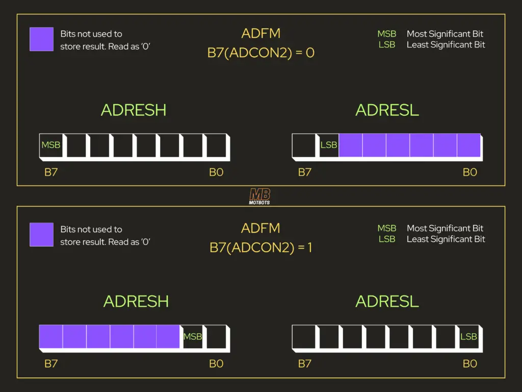
Result Formatting
On the PIC18F4525, the ADC produces a 10-bit result, but the PIC is an 8-bit microcontroller. So where do those 10 bits go?
They are split across two 8-bit registers:
- ADRESH (high byte)
- ADRESL (low byte)
How those 10 bits are arranged inside those two registers depends on something called result formatting (justification).
Result formatting determines whether the 10-bit ADC result is:
- right-justified
- left-justified
This is controlled by the ADFM bit in the ADCON2 register. If the ADFM is 1:
\begin{equation}
\text{ADFM}\:=\:1
\end{equation}
The 10-bit result is aligned to the right side of the 16-bit space. The bit layout would look something like the following:
\begin{equation}
\text{ADRESH:}\:\text{000000RR}
\end{equation}
\begin{equation}
\text{ADRESL:}\:\text{RRRRRRRR}
\end{equation}
Where R is the ADC result bits. In other words, the lower 8 bits go in ADRESL, and the upper 2 bits go into the lowest bits of ADRESH.
For example, let’s say that the ADC result is 512:
\begin{equation}
512\:=\:1000000000\text{ (10-bit)}
\end{equation}
How we did this is as follows:
| Powers of 2 | Binary (10-bit) | Conversion | ADC Result |
| 29 28 27 26 25 24 23 22 21 20 | 1000000000 | 29 + 0 + 0 + 0 + 0 + 0 + 0 + 0 + 0 + 0 = 512 | 512 |
So, the 10-bit value we found above, is stored as:
\begin{equation}
\text{ADRESH}\:=\:00000010
\end{equation}
\begin{equation}
\text{ADRESL}\:=\:00000000
\end{equation}
To reconstruct the full value in code, we’d write:
result = (ADRESH << 8) | ADRESL;This produces the full 10-bit number.
The reason why right-justification is popular is because it makes it easy to combine into a 16-bit variable. You don’t have to shift bits around and most applications use this format.
Let’s take a look at the key differences between the Arduino Uno — the microcontroller we studied in the previous section of this sub-series (Section 1) — and the PIC18F4525, in the table below.
Key Differences Between the Arduino Uno and PIC18F4525 (ADC)
| Feature | Arduino Uno (ATmega328P) | PIC18F4525 |
| Resolution | 10-bit resolution (0–1023). Fixed in standard Arduino core. | 10-bit resolution (0–1023). Configurable result formatting (left or right justified). |
| Ease of Use | Extremely simple. analogRead(pin) handles setup and conversion automatically. | Manual configuration required. Must set ADCON registers, select channel, start conversion, and read result. |
| Channel Configuration | Channels selected by passing a pin number to analogRead(). Arduino core manages mux settings internally. | Channel selected manually using ADCON0bits.CHS. Programmer must ensure proper analog/digital configuration via ADCON1. |
| Acquisition Control | Hidden from the user. Acquisition time and ADC clock handled automatically by Arduino core. | Must explicitly configure acquisition time (ACQT bits) and ADC conversion clock (ADCS bits). Must allow settling time before conversion. |
| Result Handling | Returns a single 10-bit integer. All bit shifting and formatting handled internally. | Result stored across two registers (ADRESH and ADRESL). Programmer must combine them properly and understand justification format. |
PWM (Pulse-Width Modulation)
Pulse-width modulation is a way to simulate an analog voltage using a digital signal. Instead of outputting a steady voltage, the pin rapidly switches (HIGH, LOW, HIGH, LOW, etc.).
Two things define a PWM signal:
- Frequency – How fast it switches
- Duty Cycle – Percentage of time signal is HIGH
For example:
- 25 percent duty cycle: LOW average voltage
- 50 percent duty cycle: Half power
- 75 percent duty cycle: Higher power
Motors and LEDs respond to the average voltage, not the switching.
PWM on PIC18F4525
Unlike the Arduino, the PIC uses dedicated CCP (Capture/Compare/PWM) modules:
- CCP1
- CCP2
PWM Hardware Structure
The PWM is built from:
- Timer2 (time base)
- PR2 (period register)
- CCPRxL (duty cycle high bits)
- CCPxCON<5:4> (duty cycle low bits)
This separation gives powerful control.
PWM Frequency Formula
The PWM period for the PIC is as follows:
\begin{equation}
\text{PWM Period}\:=\:\text{[(PR2 + 1)}\;\text{x}\;4\;\text{x}\;T_{OSC}\;\text{x}\;\text{TMR2 prescaler]}
\end{equation}
Where:
\begin{equation}
T_{OSC}\:=\:\frac{1}{F_{OSC}}
\end{equation}
This gives direct control over frequency. Unlike an Arduino, a PIC does not lock you into predefined values.
PWM Resolution
The resolution for a PIC depends on the PR2 (period register) and prescaler. The maximum PWM resolution is up to 10-bit resolution (matches ADC resolution). This is higher than Arduino’s default 8-bit PWM.
Duty Cycle Calculation
The duty cycle value is given by:
\begin{equation}
\text{Duty Cycle}\:=\:(\text{CCPRxL:CCPxCON<5:4>})
\end{equation}
This expression is showing how the PIC stores a 10-bit PWM duty cycle value inside hardware registers.
The colon : means “Combine these bits together.” So we are forming one 10-bit number from two different places.
Where the 10 Bits Come From
The PIC18F4525 PWM module stores the duty cycle like this:
| Bits | Stored In |
| Upper 8 bits | CCPRxL register |
| Lower 2 bits | CCPxCON<5:4> bits (DCxB1:DCxB0) |
So the full 10-bit duty value is:
[ CCPRxL (8 bits) ][ CCPxCON<5:4> (2 bits) ]That’s what this notation means:
CCPRxL : CCPxCON<5:4>It’s a 10-bit number split across two registers.
🤔 Why Is It Split Like This?
Because the PWM module is designed to support 10-bit resolution, but the registers are only 8 bits wide.
So Microchip stores:
- The top 8 bits in one register
- The bottom 2 bits in control bits
That gives:
\begin{equation}
2^{10}\:=\:1024\text{ possible duty cycles}
\end{equation}
Range:
0 → 1023Practical Example
Let’s say your ADC reading is:
512Binary form (10-bit):
1000000000Now the hardware splits it:
- Upper 8 bits → 10000000 → goes into CCPRxL
- Lower 2 bits → 00 → goes into CCPxCON<5:4>
Together, they reconstruct the full 10-bit duty.

How Your Code Handles It
Your function does exactly this:
CCPR1L = (uint8_t)(duty10 >> 2); // upper 8 bits
CCP1CONbits.DC1B = (uint8_t)(duty10 & 0x3); // lower 2 bits- >> 2 shifts off the lower 2 bits → gives upper 8 bits
- & 0x3 masks out everything except the lower 2 bits
That perfectly matches:
CCPRxL : CCPxCON<5:4>How This Relates to Duty Cycle Percentage
The 10-bit number determines how long the PWM output stays HIGH during one cycle.
If:
Duty = 0→ 0 percent (always LOW)
If:
Duty = 512→ ~50 percent
So the register expression represents the raw duty count, not the percentage directly.
For example, if full-scale is 1023:
- 256 = ~25 percent duty cycle
- 512 = ~50 percent duty cycle
- 768 = ~75 percent duty cycle
This aligns nicely with ADC resolution.
Example Setup Flow
To configure the PWM on a PIC, you perform the following steps:
- Configure CCP module in PWM mode
- Configure Timer2 prescaler
- Set PR2 (defines frequency)
- Load duty cycle value
- Enable Timer2
This is more steps than the Arduino, but there’s more control using the PIC.
Let’s take a look at the key differences between the Arduino Uno — the microcontroller we studied in the previous section of this sub-series (Section 1) — and the PIC18F4525, in the table below.
Key Differences Between the Arduino Uno and PIC18F4525 (PWM)
| Feature | Arduino Uno (ATmega328P) | PIC18F4525 |
| Ease of Use | Very simple. analogWrite(pin, value) sets PWM with one function call. | Manual setup required. Must configure CCP module, Timer2, prescaler, PR2 value, and duty registers. |
| Resolution | 8-bit PWM by default (0–255). | 10-bit PWM resolution (0–1023) using CCP module. |
| Frequency Control | PWM frequency is preset by Arduino core (varies by pin). Changing it requires direct timer manipulation. | PWM frequency fully programmable via Timer2 prescaler and PR2 register. User calculates exact frequency. |
| Hardware Structure | PWM tied to specific timer hardware, abstracted by Arduino core. | Dedicated CCP (Capture/Compare/PWM) modules tied to Timer2. Explicit hardware configuration required. |
| Flexibility | Great for quick LED dimming and simple motor control. Limited unless you modify timer registers manually. | High flexibility. User controls resolution, frequency, timing source, and behavior at the register level. |

Interrupts
An interrupt is a hardware-triggered event that temporarily pauses normal program execution so the microcontroller can respond immediately.
Instead of constantly checking (polling):
if (buttonPressed) { ... }The hardware says, “Stop what you’re doing. Handle this now.” Then, the MCU saves the current execution state, jumps to a special function, executes it, then returns to where it left off. This special function is called an ISR (Internal Service Routine).
Interrupts on PIC18F4525
The PIC18F4525 provides a more configurable interrupt system.
Interrupt Types
The PIC18F4525 MCU includes the following interrupts:
- External interrupts (INT0, INT1, INT2)
- Timer interrupts (TMR0, TMR1, TMR2, TMR3)
- ADC interrupt
- UART interrupt
- CCP interrupts
- Port change interrupt
- EEPROM write interrupt
Interrupt Priority
The interrupt priority on a PIC is a major feature. The PIC18F4525 supports:
- High-priority interrupts
- Low-priority interrupts
This is something Arduino (ATmega328P) does not provide in the same way. This allows critical real-time events to preempt lower ones. For example:
- Motor safety interrupt = high priority
- Temperature update interrupt = low priority
Enabling Interrupts
Interrupt configuration for a PIC requires:
- Enable specific interrupt source
- Clear interrupt flag
- Enable peripheral interrupt
- Enable global interrupt
An example flow of this in code would be as follows:
INTCONbits.GIE = 1; // Global enable
INTCONbits.PEIE = 1; // Peripheral enable
INTCONbits.TMR0IE = 1; // Enable Timer0 interruptThis is much more manual than for an Arduino.
ISR Structure
A typical ISR for a PIC in code is as follows:
void __interrupt() ISR(void) {
    if (INTCONbits.TMR0IF) {
        LATBbits.LATB0 ^= 1;
        INTCONbits.TMR0IF = 0;
    }
}You must manually check which interrupt occurred and manually clear interrupt flags. This is unlike Arduino, where vector automatically routes to correct ISR.
Let’s take a look at the key differences between the Arduino Uno — the microcontroller we studied in the previous section of this sub-series (Section 1) — and the PIC18F4525, in the table below.
Key Differences Between the Arduino Uno and PIC18F4525 (Interrupts)
| Feature | Arduino Uno (ATmega328P) | PIC18F4525 |
| Abstraction | High-level abstraction. attachInterrupt() simplifies setup and hides register details. | Low-level control. Programmer directly enables interrupt bits and manages flags in registers (INTCON, INTCON2, PIE, PIR, etc.). |
| Priority Levels | No built-in priority levels in the standard Arduino core. All interrupts effectively treated the same. | Supports optional high and low priority interrupt levels (when enabled). Allows more advanced control of interrupt handling order. |
| ISR Vectoring | Simplified ISR syntax using Arduino core. Hardware vectoring is hidden from user. | Single interrupt vector (or high/low vectors if priority enabled). Programmer must manually check and clear individual interrupt flags inside ISR. |
| Configuration | Edge selection and pin mapping handled internally when using attachInterrupt(). | Must configure edge selection bits (e.g., INTEDG0), enable interrupt bits, and clear flags manually. |
| Learning Curve | Easier for beginners. Focus is on responding to events rather than understanding hardware. | Steeper learning curve. Encourages understanding of interrupt flags, vectoring, priorities, and timing behavior. |
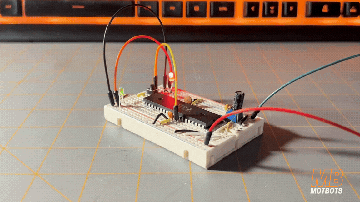
PIC18F4525 Microcontroller Demonstration
Now that we have a general idea of some of the features of a microcontroller, especially for the PIC18F4525, I believe the best way to really learn is by doing.
Below is a very simple, beginner-friendly “Microcontroller 101” mini-project for an PIC18F4525 that touches upon the GPIO, Timer and Delay, ADC, PWM, and Interrupts in a way that’s easy to understand.
At a system level, the circuit will demonstrate an analog-controlled PWM output with interrupt-driven scheduling and enable/disable button.
The idea of the project is as follows:
- A potentiometer creates an analog voltage and the ADC reads it
- That ADC value sets an LED brightness providing a PWM output
- A button triggers instantly and an external interrupt toggles “enabled/disabled”
- A timer interrupt runs periodically which sets a flag to do work (non-blocking)
In plain terms:
- You’ll turn a knob (or change a voltage on AN0).
- The PIC will read that voltage using the ADC
- It will convert that value directly into a PWM duty cycle.
- The PWM signal will drive something (LED brightness).
- A button on RB0 will toggle the system ON/OFF.
- A heartbeat LED will blink to show the microcontroller is alive.
Important Information to Know
Before continuing on to the PIC18F4525 microcontroller demonstration circuit, it’s best that you first review the following topics, so that you know how to perform the circuit and coding setup that’s involved when using a PIC microcontroller:
- What you’ll need to program the PIC18F4525
- Using a PICkit 3 in-circuit debugger / programmer
- About the PIC18F4525
- How to setup Microchip’s MPLAB X software
- Things you need to know in the C programming language
- Getting familiar with the hexadecimal system
You may find all this information and more at our articled titled, “Introduction to PIC Programming Using C: Programming a Super Simple LED Switch – Part 1: The Preliminaries.”

Parts List
Below are the items we’ll need to assemble our PIC circuit, as well as the schematic diagram we’ll need to guide us in creating the circuit:
| Item | Quantity |
| Microchip PIC18F4525 | 1 |
| Solderless Breadboard | 1 |
| 5V regulated supply | 1 |
| 10k trimmer potentiometer | 1 |
| Green LED | 1 |
| Red LED (heartbeat/status LED) | 1 |
| 220Ω resistor | 2 |
| 10kΩ pull-up resistors | 2 |
| 10µF electrolytic capacitor | 1 |
| 0.1µF decoupling capacitor | 4 |
| Momentary push-button switch | 1 |
| Jumper Wires | Various colors and sizes |
Schematic Diagram of PIC18F4525 Microcontroller Demo
The following image is a schematic diagram of the mini-project we’re performing showing the Microchip PIC18F4525 microcontroller in circuit with connected components as should be done when making your prototype circuit.

Microchip PIC18F4525 Datasheet
I’ve provided the datasheet from Microchip for the PIC18F4525, below. You may obtain this datasheet directly from Microchip’s website here, or you may download the datasheet by clicking on the image below.
Breadboard Assembly
For this demonstration, I will be using a 400-point breadboard for its small size, since this is a mini-project that uses few components. You may use any size you’d like.

A Helpful Tip (Marking the PIC)
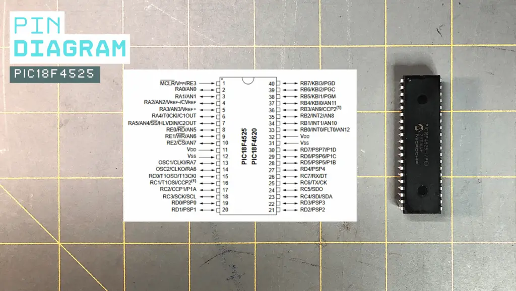
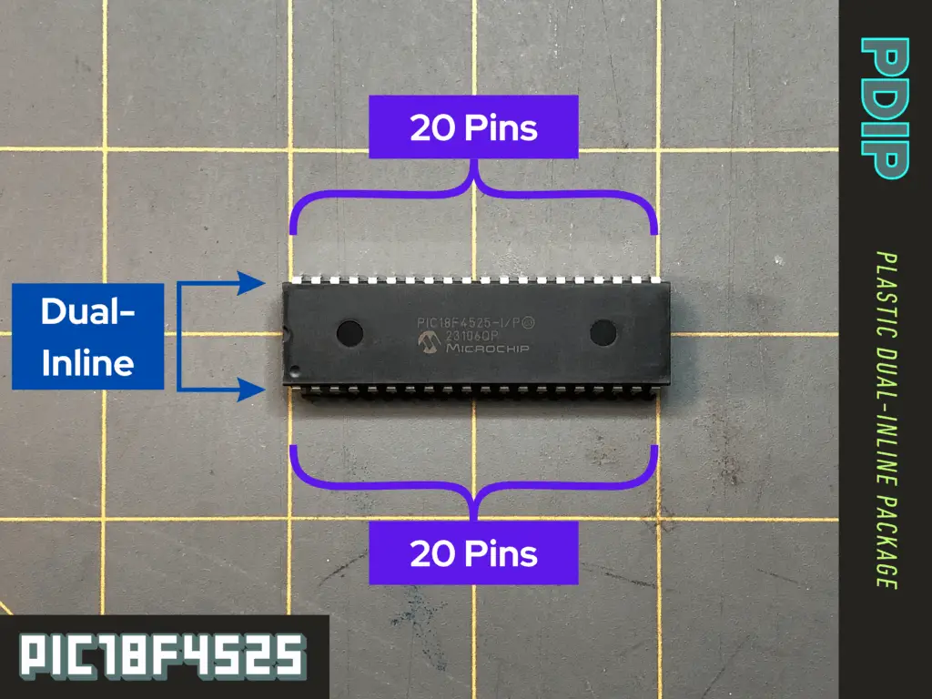
For this project, we’re using a dual-inline package (PDIP) for the PIC18F4525. The first “P” in PDIP stands for plastic. This means that the 40 pins that our PIC has is divided in two (dual) and are lined (in-line) on both the long sides of the PIC’s body (package).
40 pins is a lot, and it can become quite tedious to count them every time we are making connections to them. Also, we’ll need to remove and replace the PIC onto the breadboard when we need to write our code to it from the universal programmer seat adapter we’re using for the PICkit 3 programmer.
See more about the universal programmer and PICkit 3 at our article titled, “Introduction to PIC Programming Using C: Programming a Super Simple LED Switch – Part 3: The Code.”
So, to make things a bit easier, before we get to prototyping our circuit on a breadboard, I find it extremely helpful to make some marks directly onto the PIC’s body before I start making connections to its pins.
First, place your PIC down on a flat surface or into a breadboard with the pins facing down. Notice the small dimple in one of the PIC’s corners. Orient the PIC so that the small dimple it has for reference is in the top-left corner when facing you. This reference dimple is there to identify pin 1 of the PIC.
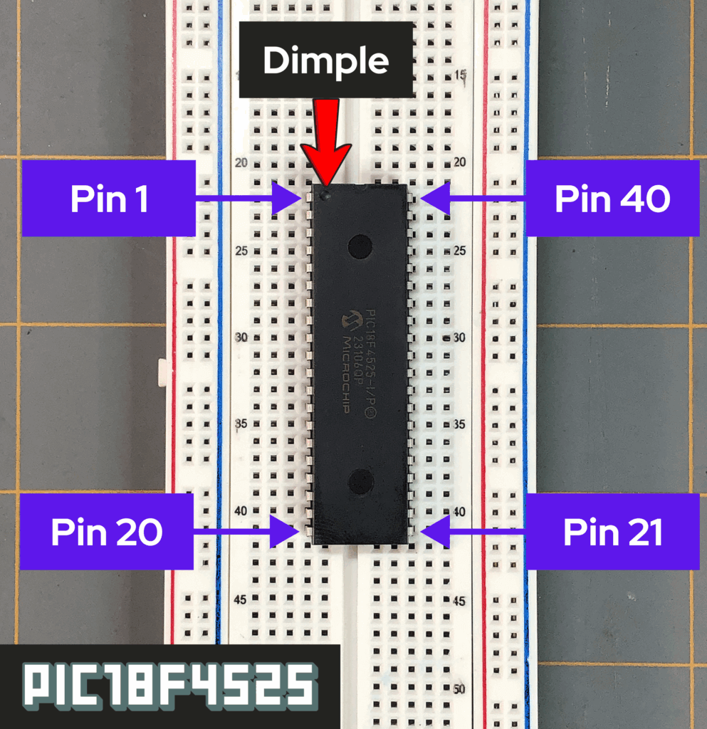
Pin 1 starts from the reference dimple in the top-left corner orientation, and the pin number sequence continues from there, the next pin being pin 2, then pin 3, and so on — down to pin 20, being the last pin on the left-hand side of the PIC.
The pin order continues on the right-hand side of the PIC, directly across from pin 20, where pin 21 begins on the bottom right-hand side of the PIC. From there, the pin number sequence continues, going on to pin 22, then to pin 23, and so on — working your way up the right-hand side of the PIC.
Now, grab yourself an ultra-fine tip permanent marker and take a look at the 40-Pin PDIP Pin Diagram for the PIC18F4525, found on page 2 of the datasheet. We see on the datasheet that pins 11 and 32 are both the VDD pins. These pins are both for the positive supply voltage for the PIC.
- Having the PIC with the top of its body facing up and the small dimple it has for reference for pin 1 in the top-left corner facing you, count to pin 11 down the left-hand side of the PIC. Make a “+” mark next to this pin directly on the body of the PIC.
- Now count up the right-hand side of the PIC to pin 32. Make a “+” mark next to this pin directly on the body of the PIC.
Looking at the Pin Diagram on the datasheet again, we see that pins 12 and 31 are both the VSS pins. These pins are both for the negative supply voltage for the PIC.
- Having the PIC with the top of its body facing up and the small dimple it has for reference for pin 1 in the top-left corner facing you, count to pin 12 down the left-hand side of the PIC. Make a “-” mark next to this pin directly on the body of the PIC.
- Now count up the right-hand side of the PIC to pin 31. Make a “-” mark next to this pin directly on the body of the PIC.
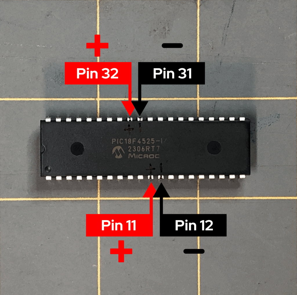
Having made these marks on the PIC’s body for the supply voltage will help in quickly placing your PIC correctly back onto the breadboard after removing it and lining up the connections you made on the breadboard. It’ll also help you quickly reference other pin numbers on the PIC from the datasheet, so that you don’t have to count so many pins all the time.
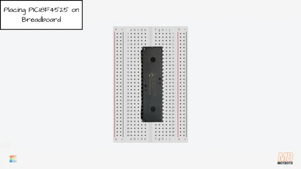
Placing the PIC18F4525 on the Breadboard
Let’s start by facing the 400-point breadboard vertically, with the letters and numbers of the breadboard’s columns and rows facing right side up.
Taking the PIC18F4525 microcontroller, I placed its pins on either side of the center gap of the breadboard to isolate each side of the microcontroller’s pins from each other. Pins 1-20 of the PIC were placed at points d6-d25 — pin 1 being at point d6 of the breadboard. Pins 21-40 of the PIC were placed at points h25-h6 of the breadboard, respectively.
Breadboard Power Supply Setup
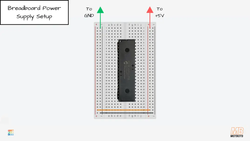
Power Supply Distribution
To allow for positive power supply distribution throughout the breadboard, I added a red jumper wire to the top point of the right-hand side positive power rail.
To continue this connection across to the left-hand side positive power rail of the breadboard, I connected an orange jumper wire to one of the bottom points of the right-hand side positive power rail across to one of the bottom points of the left-hand side positive power rail.
To allow for negative power supply distribution throughout the breadboard, I added a green jumper wire to the top point of the left-hand side negative power rail.
To continue this connection across to the right-hand side negative power rail of the breadboard, I connected a black jumper wire to the bottom point of the left-hand side negative power rail across to the bottom point of the right-hand side negative power rail.
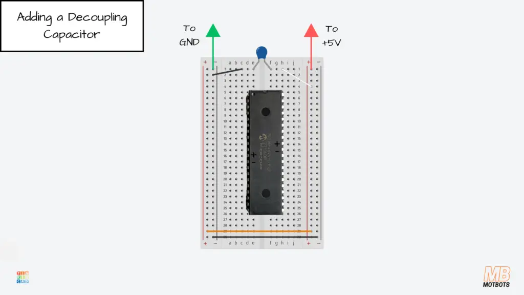
Adding a Decoupling Capacitor
We are going to place a small 0.1µF ceramic capacitor across the main 5V and GND rails of the breadboard.
I took a 0.1µF capacitor and placed its pins at points e1 and f1, across the center gap of the breadboard. To make the connections of the pins of the cap to the positive and negative rails, I did the following:
- I connected a small white jumper wire at point h1 — inline with the leg of the capacitor at point f1.
- I connected the other end of the white jumper into a point at the adjacent side positive power rail.
- I connected a small black jumper wire at point c1 — inline with the leg of the capacitor at point e1.
- I connected the other end of the black jumper into a point at the adjacent side negative power rail.
This capacitor will act as a decoupling capacitor which will handle very fast, high frequency spikes, as well as suppress switching noise from the MCU.
The 0.1 µF reacts extremely quickly but stores much less charge.
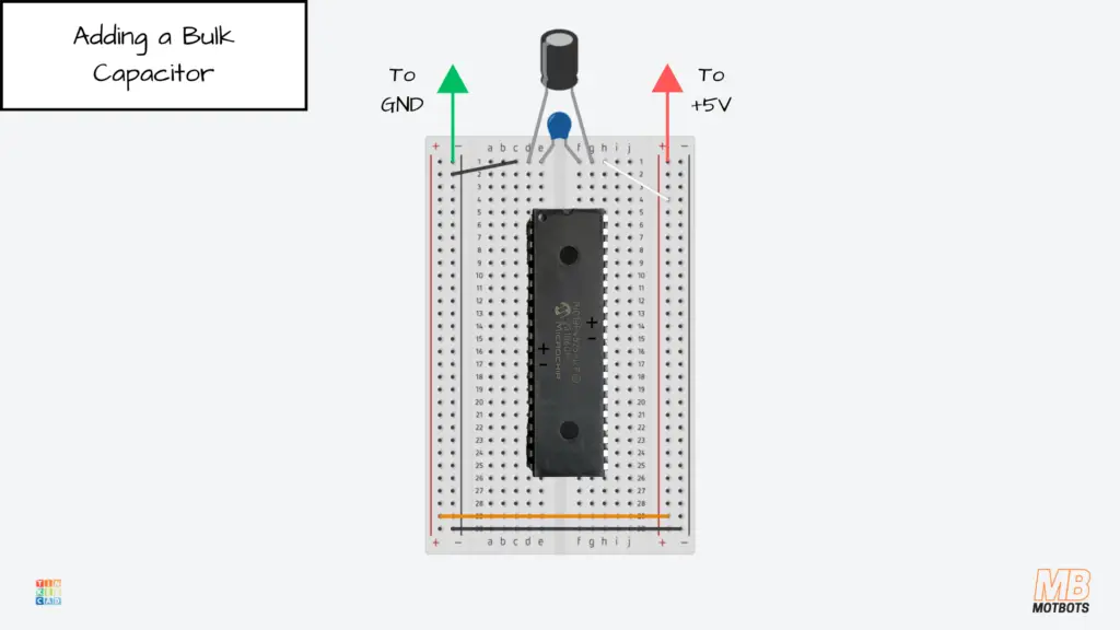
Adding a Bulk Capacitor
We are going to place another capacitor across the main 5V and GND rails of the breadboard. This next capacitor will be a 10µF electrolytic capacitor.
I took a 10µF capacitor and placed its pins at points d1 and g1, across the center gap of the breadboard. The legs of this capacitor are directly across the decoupling capacitor we just placed across the main 5V and GND rails.
- The anode of the 10µF cap is at point g1 — inline with the leg of the decoupling cap’s leg at point f1, as well as the white jumper wire that connects to the positive power rail.
- The cathode of the 10µF cap is at point d1 — inline with the leg of the decoupling cap’s leg at point e1, as well as the black jumper wire that connects to the negative power rail.
This capacitor will act as a bulk capacitor which will handle slower, larger current changes across the power rails, stabilizing the rails overall when the load changes.
The bulk capacitor reacts slowly but stores more charge.
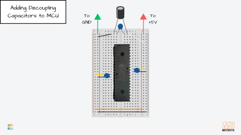
Adding Decoupling Capacitors to the MCU
We are going to place 0.1µF ceramic capacitors very close to the microcontroller’s VDD and VSS pins. Remember, there’s VDD and VSS pins on both sides of the PIC18F4525:
- VDD: pins 11 and 32
- VSS: pins 12 and 31
I took one 0.1µF ceramic capacitor and placed its pins at points c16 and c17 on the breadboard — inline with the VDD and VSS pins (pins 11 and 12) of the PIC.
To continue the connections of the VDD and VSS pins (pins 11 and 12) to the power rails:
- I connected a small yellow jumper wire to point b16 — inline with pin 11 (VDD) of the MCU, and placed the other end of the jumper wire into a point at the adjacent positive supply rail.
- I connected a small black jumper wire to point a17 — inline with pin 12 (VSS) of the MCU, and placed the other end of the jumper wire into a point at the adjacent negative supply rail.
Next, I took another 0.1µF ceramic capacitor and placed its pins at points i14 and i15 on the breadboard — inline with the VDD and VSS pins (pins 32 and 31) of the PIC.
To continue the connections of the VDD and VSS pins (pins 32 and 31) to the power rails:
- I connected a small yellow jumper wire to point j14 — inline with pin 32 (VDD) of the MCU, and placed the other end of the jumper wire into a point at the adjacent positive supply rail.
- I connected a small black jumper wire to point j15 — inline with pin 31 (VSS) of the MCU, and placed the other end of the jumper wire into a point at the adjacent negative supply rail.
The capacitors are considered local decoupling capacitors. Their job is to:
- Absorb very fast, tiny current spikes
- Smooth out high-frequency noise
- Prevent the PIC from glitching or resetting
They respond to rapid switching noise inside the chip.
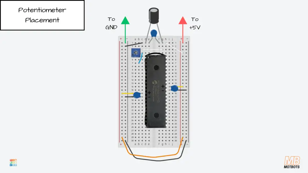
Potentiometer Placement
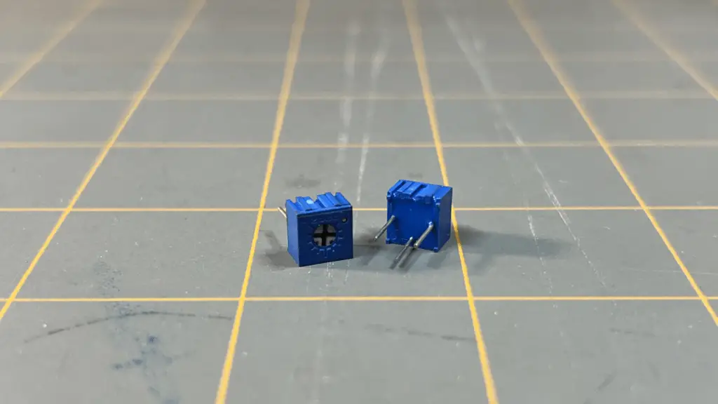
For this PIC project demonstration we’ll be using a 10kΩ trimmer potentiometer.
I placed my trimpot’s terminals at points a3, b4, and a5, on the breadboard — the center terminal or wiper of the trimpot being at point b4.
I connected a short blue jumper wire from point c4 — inline with the wiper of the trimpot — to pin 2 (AN0) of the PIC18F4525, at point b7 on the breadboard.
Next, I connected a short white jumper wire from point c3 — inline with one outside pin of the trimpot, to point g3, across the center gap of the breadboard. Then, I took another short white jumper wire to connect from point i3, to a point on the adjacent positive power supply rail on the breadboard.
To finish up the connections for the trimpot, I connected a small black jumper wire from the point d5 — inline with the other outside pin of the trimpot to point h5, across the center gap of the breadboard. Finally, I took another short black jumper wire to connect from point j5, to a point on the adjacent negative power supply rail of the breadboard.
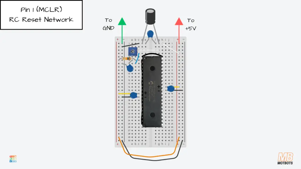
Pin 1 (MCLR) RC Reset Network
The MCLR pin (Master Clear Reset) on the PIC18F4525 is the microcontroller’s external reset input.
If this pin is pulled low, the PIC immediately resets. If it is held high, the PIC runs normally.
If we don’t initially tie the MCLR pin firmly to a known logic level, this will allow it to “float,” meaning it could randomly pick up electrical noise or even react when the breadboard is touched.
Initially, I didn’t tie the MCLR pin to anything and the results of my circuit became unpredictable resets and unstable behavior, like LEDs flickering or going out completely.
To alleviate these issues, I connected a 10kΩ pull-up resistor at the point b6 — inline with the MCLR pin (pin 1) of the MCU, to a point at the adjacent positive supply rail.
Next, I connected a 0.1µF ceramic capacitor at the point a6 — inline with the MCLR pin (pin 1) of the MCU, to a point at the adjacent negative supply rail.
10kΩ Resistor — The Pull-Up Resistor
The 10kΩ resistor connects MCLR to +5V. This is called the pull-up resistor. It’s job is to:
- Hold MCLR at a steady HIGH level
- Prevent the pin from floating
- Ensure the PIC stays out of reset
The pull-up resistor keeps the reset pin in the “run” state unless something intentionally pulls it low.
0.1µF Capacitor — The Reset Filter / RC Delay Capacitor
The 0.1µF capacitor connects MCLR to ground.
This capacitor works together with the 10kΩ resistor to form what’s called an RC reset network.
This small capacitor:
- Filters out electrical noise
- Prevents brief voltage spikes from resetting the PIC
- Creates a short delay at power-up
The capacitor makes reset behavior smooth and stable instead of glitchy.
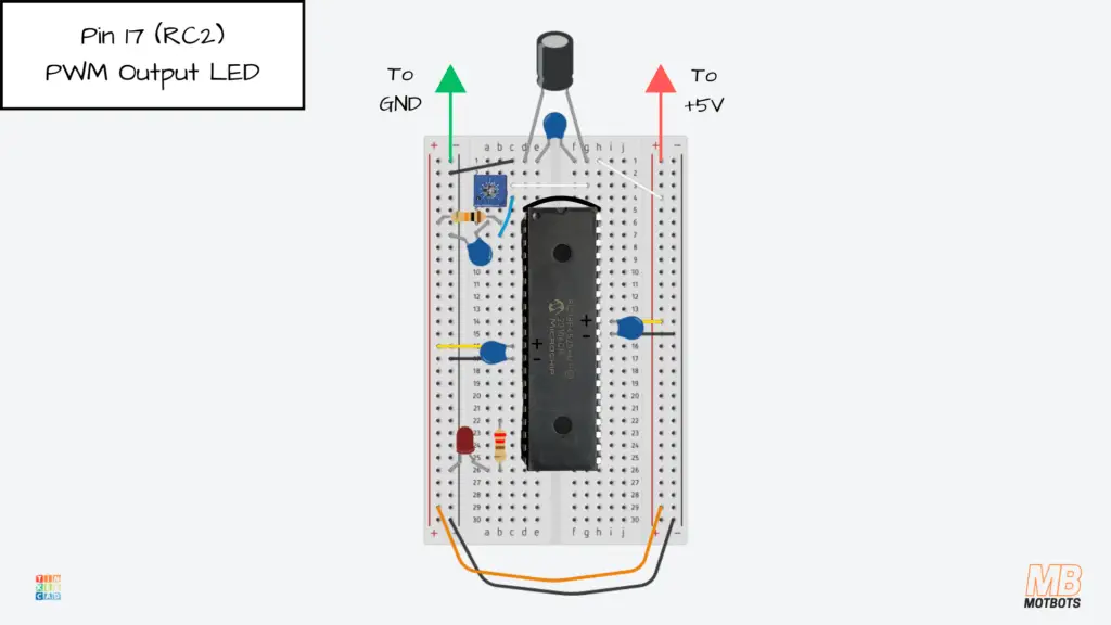
Pin 17 (RC2) PMW Output LED
The PWM output LED, also called:
- Dimming LED
- Control LED
- Output LED
- PWM-Controlled LED
has its brightness controlled by an ADC reading from the potentiometer. This demonstrates analog to digital to PWM control. It also represents a power-controlled load (could later become a fan, motor, etc.).
I connected a 220Ω current-limiting resistor for the red LED I’m using as my output LED from the point b22 — inline with pin 17 (RC2) of the MCU, to point b26.
I connected the red LED’s anode (+) at point a26 — inline with the 220Ω resistor’s leg at point b26, then connected the LED’s cathode (-) to a point at the adjacent negative supply rail.
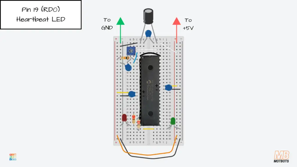
Pin 19 (RD0) Heartbeat LED
The heartbeat LED, also called:
- Indicator LED
- System Indicator
- Status LED
blinks slowly to show the microcontroller is “alive.” This LED confirms that the Timer0 interrupt is running and acts as a visual “system OK” indicator.
I connected a 220Ω current-limiting resistor for the green LED I’m using as my indicator LED from the point c24 — inline with pin 19 (RD0) of the MCU, to point c27.
Next, I connected a small yellow jumper wire from point e27 to point f27 — bridging across the center gap of the breadboard.
I connected the green LED’s anode (+) at point j27 — inline with the yellow jumper wire at point f27, then connected the green LED’s cathode (-) to a point at the adjacent negative supply rail.
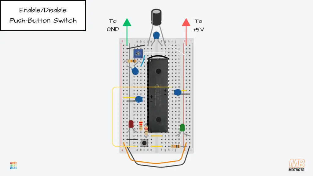
Enable/Disable Push-Button Placement
The push-button switch or enable/disable button, also called:
- System Enable Switch
- Output Enable Button
- INT0 Button (hardware reference)
- Toggle Control Button
when pressed, triggers the INT0 interrupt. The interrupt service routine toggles:
g_enabled = !g_enabled;The system either allows PWM output or forces the PWM output to zero.
The button acts as a master ON/OFF control for the PWM system.
I placed my two-terminal push-button switch across the points c28 and c30.
I connected a small black jumper wire at point a28 — inline with the pin of the push-button at point c28, to a point in the adjacent negative supply rail.
I then connected a small yellow jumper wire across the center gap of the breadboard at points e30 and f30 — inline with the pin of the push-button switch at point c30. I continued that connection using a 10kΩ pull-up resistor, placing its pins at point h30, to a point at the adjacent positive power rail.
Now’s the time to complete the connection from pin 33 (RB0) of the MCU to the push-button switch. How I did this was that I connected a long yellow jumper wire from the point i13 — inline with pin 33 (RB0) of the PIC, to point a30 — inline with with the pin of the push-button switch at point c30.
The toggle control button, at this point, is:
- Connected to RB0
- Able to use the INT0 external interrupt
- Configured for falling-edge detection
- Equipped with a pull-up resistor to +5V
Code for PIC18F4525 Microcontroller Demo
This program turns the PIC18F4525 into a tiny control system:
- A potentiometer creates a changing voltage on AN0 (RA0)
- The PIC reads that voltage using the ADC
- That ADC number becomes a PWM duty cycle on CCP1 (RC2) (dimming an LED)
- A button on RB0 (INT0) toggles the output enabled / disabled
- A “heartbeat” LED blinks slowly so you can see the code is still running
The code is as follows:
/******************************************************************************
*
* File: PIC-101.c
* Author: Dustin Hodges (Motbots)
* Microcontroller: PIC18F4525
* Date: 02/25/2026
*
* Project: A basic program for a beginner-friendly Microcontroller 101
* mini-project for a PIC18F4525 microcontroller that touches upon the GPIO,
* Timer and Delay, ADC, PWM, and Interrupts in a way that's easy to understand.
*
* RA0 --> Potentiometer wiper
* RB0 --> Push-button Switch (SW1) and Pull-up Resistor (R2)
* RC2 --> Green LED (D1)
* RD0 --> Red Status LED (D2)
*
* Last Updated on March 2, 2026, 6:01 PM
******************************************************************************/
// PIC18F4525 Configuration Bit Settings
// 'C' source line config statements
// CONFIG1H
#pragma config OSC = INTIO67 // Oscillator Selection bits (Internal oscillator block, port function on RA6 and RA7)
#pragma config FCMEN = OFF // Fail-Safe Clock Monitor Enable bit (Fail-Safe Clock Monitor disabled)
#pragma config IESO = OFF // Internal/External Oscillator Switchover bit (Oscillator Switchover mode disabled)
// CONFIG2L
#pragma config PWRT = OFF // Power-up Timer Enable bit (PWRT disabled)
#pragma config BOREN = SBORDIS // Brown-out Reset Enable bits (Brown-out Reset enabled in hardware only (SBOREN is disabled))
#pragma config BORV = 3 // Brown Out Reset Voltage bits (Minimum setting)
// CONFIG2H
#pragma config WDT = OFF // Watchdog Timer Enable bit (WDT disabled (control is placed on the SWDTEN bit))
#pragma config WDTPS = 32768 // Watchdog Timer Postscale Select bits (1:32768)
// CONFIG3H
#pragma config CCP2MX = PORTC // CCP2 MUX bit (CCP2 input/output is multiplexed with RC1)
#pragma config PBADEN = ON // PORTB A/D Enable bit (PORTB<4:0> pins are configured as analog input channels on Reset)
#pragma config LPT1OSC = OFF // Low-Power Timer1 Oscillator Enable bit (Timer1 configured for higher power operation)
#pragma config MCLRE = ON // MCLR Pin Enable bit (MCLR pin enabled; RE3 input pin disabled)
// CONFIG4L
#pragma config STVREN = ON // Stack Full/Underflow Reset Enable bit (Stack full/underflow will cause Reset)
#pragma config LVP = OFF // Single-Supply ICSP Enable bit (Single-Supply ICSP disabled)
#pragma config XINST = OFF // Extended Instruction Set Enable bit (Instruction set extension and Indexed Addressing mode disabled (Legacy mode))
// CONFIG5L
#pragma config CP0 = OFF // Code Protection bit (Block 0 (000800-003FFFh) not code-protected)
#pragma config CP1 = OFF // Code Protection bit (Block 1 (004000-007FFFh) not code-protected)
#pragma config CP2 = OFF // Code Protection bit (Block 2 (008000-00BFFFh) not code-protected)
// CONFIG5H
#pragma config CPB = OFF // Boot Block Code Protection bit (Boot block (000000-0007FFh) not code-protected)
#pragma config CPD = OFF // Data EEPROM Code Protection bit (Data EEPROM not code-protected)
// CONFIG6L
#pragma config WRT0 = OFF // Write Protection bit (Block 0 (000800-003FFFh) not write-protected)
#pragma config WRT1 = OFF // Write Protection bit (Block 1 (004000-007FFFh) not write-protected)
#pragma config WRT2 = OFF // Write Protection bit (Block 2 (008000-00BFFFh) not write-protected)
// CONFIG6H
#pragma config WRTC = OFF // Configuration Register Write Protection bit (Configuration registers (300000-3000FFh) not write-protected)
#pragma config WRTB = OFF // Boot Block Write Protection bit (Boot Block (000000-0007FFh) not write-protected)
#pragma config WRTD = OFF // Data EEPROM Write Protection bit (Data EEPROM not write-protected)
// CONFIG7L
#pragma config EBTR0 = OFF // Table Read Protection bit (Block 0 (000800-003FFFh) not protected from table reads executed in other blocks)
#pragma config EBTR1 = OFF // Table Read Protection bit (Block 1 (004000-007FFFh) not protected from table reads executed in other blocks)
#pragma config EBTR2 = OFF // Table Read Protection bit (Block 2 (008000-00BFFFh) not protected from table reads executed in other blocks)
// CONFIG7H
#pragma config EBTRB = OFF // Boot Block Table Read Protection bit (Boot Block (000000-0007FFh) not protected from table reads executed in other blocks)
// #pragma config statements should precede project file includes.
// Use project enums instead of #define for ON and OFF.
#include <xc.h>
#include <stdbool.h>
#include <stdint.h>
#define _XTAL_FREQ 8000000UL // Must match OSCCON setting
// ====== Pin ideas ======
#define HEARTBEAT_LAT LATDbits.LATD0
#define HEARTBEAT_TRIS TRISDbits.TRISD0
volatile bool g_enabled = true;
volatile bool g_tickFlag = false;
// ---------- Helpers ----------
static void adc_init(void) {
// PIC18F4525: ADCON1 controls analog/digital selection.
// 0x0E is a very common beginner setting: AN0 = analog, all others digital.
// Vref+ = VDD, Vref- = VSS
ADCON1 = 0x0E;
// ADCON2:
// ADFM=1 (right-justified)
// ACQT=010 (4 TAD acquisition time)
// ADCS=110 (Fosc/64)
ADCON2 = 0xAE; // 0b10101110
ADCON0 = 0;
ADCON0bits.CHS = 0; // AN0
ADCON0bits.ADON = 1; // ADC ON
}
static uint16_t adc_read_an0(void) {
ADCON0bits.CHS = 0; // AN0
__delay_us(10); // acquisition delay
ADCON0bits.GO = 1;
while (ADCON0bits.GO); // wait
return ((uint16_t)ADRESH << 8) | ADRESL; // 0..1023 (right-justified)
}
static void pwm_ccp1_init(uint16_t pwm_hz) {
// CCP1 PWM output is on RC2
TRISCbits.TRISC2 = 0;
// Timer2 prescale = 16
T2CONbits.T2CKPS = 0b11;
// PR2 = (Fosc/(4*prescale*pwm_hz)) - 1
const uint32_t prescale = 16UL;
uint32_t pr2 = (_XTAL_FREQ / (4UL * prescale * (uint32_t)pwm_hz)) - 1UL;
if (pr2 > 255UL) pr2 = 255UL;
PR2 = (uint8_t)pr2;
// CCP1 PWM mode
CCP1CONbits.CCP1M = 0b1100;
// Start Timer2
T2CONbits.TMR2ON = 1;
}
static void pwm_ccp1_set_duty_10bit(uint16_t duty10) {
if (duty10 > 1023) duty10 = 1023;
CCPR1L = (uint8_t)(duty10 >> 2);            // upper 8 bits
CCP1CONbits.DC1B = (uint8_t)(duty10 & 0x3); // lower 2 bits
}
static void timer0_init_periodic(void) {
// Timer0: 16-bit, Fosc/4, prescaler 1:256
// With Fosc=8MHz => instruction clock = 2MHz => tick = 0.5us
// Prescaled tick = 0.5us * 256 = 128us per Timer0 increment
// Overflow (65536 counts) ~ 8.388s if starting from 0.
//
// For a ~16.384ms tick: preload so it overflows after 128 counts:
// 128 * 128us = 16.384ms
// preload = 65536 - 128 = 65408 = 0xFF80
T0CONbits.T08BIT = 0; // 16-bit
T0CONbits.T0CS = 0; // internal clock (Fosc/4)
T0CONbits.PSA = 0; // prescaler enabled
T0CONbits.T0PS = 0b111; // 1:256
// Preload for ~16.384ms tick at 8 MHz
TMR0H = 0xFF;
TMR0L = 0x80;
INTCONbits.TMR0IF = 0;
INTCONbits.TMR0IE = 1;
T0CONbits.TMR0ON = 1;
}
static void int0_init(void) {
TRISBbits.TRISB0 = 1; // RB0 input
INTCON2bits.INTEDG0 = 0; // falling edge (button to GND w/ pull-up)
INTCONbits.INT0IF = 0;
INTCONbits.INT0IE = 1;
}
// ---------- Interrupt Service Routine ----------
void __interrupt() isr(void) {
if (INTCONbits.INT0IF) {
g_enabled = !g_enabled;
INTCONbits.INT0IF = 0;
}
if (INTCONbits.TMR0IF) {
// Reload first so the period stays consistent
TMR0H = 0xFF;
TMR0L = 0x80;
g_tickFlag = true;
INTCONbits.TMR0IF = 0;
}
}
void main(void) {
// ---- Clock: make _XTAL_FREQ truthful ----
OSCCONbits.IRCF = 0b111; // 8 MHz
OSCCONbits.SCS = 0b10; // internal oscillator
// GPIO (heartbeat LED)
HEARTBEAT_TRIS = 0;
HEARTBEAT_LAT = 0;
// Init peripherals
adc_init();
pwm_ccp1_init(1000); // ~1 kHz PWM on CCP1 (RC2)
int0_init();
timer0_init_periodic();
// Enable interrupts
INTCONbits.PEIE = 1;
INTCONbits.GIE = 1;
while (1) {
if (g_tickFlag) {
g_tickFlag = false;
static uint8_t hb_div = 0;
if (++hb_div >= 30) { // adjust number for speed
hb_div = 0;
HEARTBEAT_LAT ^= 1;
}
if (g_enabled) {
uint16_t adc = adc_read_an0(); // 0..1023
// ---- Dead zone clamp ----
if (adc < 30) adc = 0; // adjust threshold if needed
pwm_ccp1_set_duty_10bit(adc); // map ADC directly to PWM duty
} else {
pwm_ccp1_set_duty_10bit(0);
}
}
}
}
This circuit reads an analog voltage from a potentiometer on AN0, converts it to a number, and uses that number to control the PWM duty cycle on RC2, while a button on RB0 enables/disables the output and a heartbeat LED shows the system is alive.
The Code Explained
Comment header
/******************************************************************************
*
* File: PIC-101.c
* Author: Dustin Hodges (Motbots)
* Microcontroller: PIC18F4525
* Date: 02/25/2026
*
* Project: A basic program for a beginner-friendly Microcontroller 101
* mini-project for a PIC18F4525 microcontroller that touches upon the GPIO,
* Timer and Delay, ADC, PWM, and Interrupts in a way that's easy to understand.
*
* RA0 --> Potentiometer wiper
* RB0 --> Push-button Switch (SW1) and Pull-up Resistor (R2)
* RC2 --> Green LED (D1)
* RD0 --> Red Status LED (D2)
*
* Last Updated on March 2, 2026, 6:01 PM
******************************************************************************/A comment block explains what the program does and has no effect on code execution.
Configuration bits
// PIC18F4525 Configuration Bit Settings
// 'C' source line config statements
// CONFIG1H
#pragma config OSC = INTIO67 // Oscillator Selection bits (Internal oscillator block, port function on RA6 and RA7)
#pragma config FCMEN = OFF // Fail-Safe Clock Monitor Enable bit (Fail-Safe Clock Monitor disabled)
#pragma config IESO = OFF // Internal/External Oscillator Switchover bit (Oscillator Switchover mode disabled)
// CONFIG2L
#pragma config PWRT = OFF // Power-up Timer Enable bit (PWRT disabled)
#pragma config BOREN = SBORDIS // Brown-out Reset Enable bits (Brown-out Reset enabled in hardware only (SBOREN is disabled))
#pragma config BORV = 3 // Brown Out Reset Voltage bits (Minimum setting)
// CONFIG2H
#pragma config WDT = OFF // Watchdog Timer Enable bit (WDT disabled (control is placed on the SWDTEN bit))
#pragma config WDTPS = 32768 // Watchdog Timer Postscale Select bits (1:32768)
// CONFIG3H
#pragma config CCP2MX = PORTC // CCP2 MUX bit (CCP2 input/output is multiplexed with RC1)
#pragma config PBADEN = ON // PORTB A/D Enable bit (PORTB<4:0> pins are configured as analog input channels on Reset)
#pragma config LPT1OSC = OFF // Low-Power Timer1 Oscillator Enable bit (Timer1 configured for higher power operation)
#pragma config MCLRE = ON // MCLR Pin Enable bit (MCLR pin enabled; RE3 input pin disabled)
// CONFIG4L
#pragma config STVREN = ON // Stack Full/Underflow Reset Enable bit (Stack full/underflow will cause Reset)
#pragma config LVP = OFF // Single-Supply ICSP Enable bit (Single-Supply ICSP disabled)
#pragma config XINST = OFF // Extended Instruction Set Enable bit (Instruction set extension and Indexed Addressing mode disabled (Legacy mode))
// CONFIG5L
#pragma config CP0 = OFF // Code Protection bit (Block 0 (000800-003FFFh) not code-protected)
#pragma config CP1 = OFF // Code Protection bit (Block 1 (004000-007FFFh) not code-protected)
#pragma config CP2 = OFF // Code Protection bit (Block 2 (008000-00BFFFh) not code-protected)
// CONFIG5H
#pragma config CPB = OFF // Boot Block Code Protection bit (Boot block (000000-0007FFh) not code-protected)
#pragma config CPD = OFF // Data EEPROM Code Protection bit (Data EEPROM not code-protected)
// CONFIG6L
#pragma config WRT0 = OFF // Write Protection bit (Block 0 (000800-003FFFh) not write-protected)
#pragma config WRT1 = OFF // Write Protection bit (Block 1 (004000-007FFFh) not write-protected)
#pragma config WRT2 = OFF // Write Protection bit (Block 2 (008000-00BFFFh) not write-protected)
// CONFIG6H
#pragma config WRTC = OFF // Configuration Register Write Protection bit (Configuration registers (300000-3000FFh) not write-protected)
#pragma config WRTB = OFF // Boot Block Write Protection bit (Boot Block (000000-0007FFh) not write-protected)
#pragma config WRTD = OFF // Data EEPROM Write Protection bit (Data EEPROM not write-protected)
// CONFIG7L
#pragma config EBTR0 = OFF // Table Read Protection bit (Block 0 (000800-003FFFh) not protected from table reads executed in other blocks)
#pragma config EBTR1 = OFF // Table Read Protection bit (Block 1 (004000-007FFFh) not protected from table reads executed in other blocks)
#pragma config EBTR2 = OFF // Table Read Protection bit (Block 2 (008000-00BFFFh) not protected from table reads executed in other blocks)
// CONFIG7H
#pragma config EBTRB = OFF // Boot Block Table Read Protection bit (Boot Block (000000-0007FFh) not protected from table reads executed in other blocks)
// #pragma config statements should precede project file includes.
// Use project enums instead of #define for ON and OFF.For a description on configuration bits, I will refer you to our article titled “Introduction to PIC Programming Using C: Programming a Super Simple LED Switch – Part 3: The Code”, where an explanation was given on configuration bits for the PIC18F4525 microcontroller.

There, you may also find an explanation on the code for that project, as well as other pertinent information on programming your PIC microcontroller, handling common errors and how to use a PICkit programmer. It’s highly recommended you review that article full of helpful resources.
There’s a whole three part series explaining how to program a PIC. Check it out at our Super Simple LED Switch Series page — a detailed series that explains the preliminaries, the PIC project, and the code.
Include headers
#include <xc.h>This line tells the compiler:
- All the register names (like PORTB, TMR0, ADCON0)
- All the individual bit names (like INTCONbits.GIE)
Without this, the compiler wouldn’t understand any of the PIC hardware names.
#include <stdbool.h>
#include <stdint.h>These are standard C libraries. They allow us to use:
- bool (true/false variables)
- uint16_t (a 16-bit unsigned number)
These make the code easier to read and safer.
Clock definition for delay functions
#define _XTAL_FREQ 8000000UL // Must match OSCCON settingXC8 delay functions like __delay_us() need to know the clock speed to calculate timing correctly. This value must match what we set later in OSCCON (8 MHz).
Repeating this statement another way, this tells the compiler “The clock speed is 8 MHz.” It is required so delay functions like:
__delay_us(10);calculate correct timing.
⚠️ Important: This must match the oscillator setting in OSCCON.
Pin shortcut names (makes code easier to read)
// ====== Pin ideas ======
#define HEARTBEAT_LAT LATDbits.LATD0
#define HEARTBEAT_TRIS TRISDbits.TRISD0Instead of typing the long register names every time, we create “nicknames”:
- HEARTBEAT_LAT controls whether RD0 is driven high or low
- HEARTBEAT_TRIS controls whether RD0 is input or output
This makes the code cleaner and easier to understand.
Variables shared with interrupts
volatile bool g_enabled = true;
volatile bool g_tickFlag = false;These are used by both the main code and the interrupt routine:
- g_enabled = whether PWM output is allowed (button toggles this)
- g_tickFlag = tells the main loop “Timer0 tick happened, do your scheduled work”
They’re marked volatile because interrupts can change them at any time.
volatile bool g_enabled = true;
volatile bool g_tickFlag = false;When a variable can change outside the normal flow of the program — like inside an interrupt — we mark it as volatile.
This tells the compiler: “Don’t assume this value stays the same. It might change at any moment.”
Without volatile, the compiler might optimize the code in a way that ignores updates from the interrupt routine — and your program wouldn’t behave correctly.
In embedded systems, volatile is essential anytime:
- An interrupt modifies a variable
- A hardware register may change unexpectedly
ADC Setup and Reading (AN0 / RA0)
adc_init()
// ---------- Helpers ----------
static void adc_init(void) {
// PIC18F4525: ADCON1 controls analog/digital selection.
// 0x0E is a very common beginner setting: AN0 = analog, all others digital.
// Vref+ = VDD, Vref- = VSS
ADCON1 = 0x0E;
// ADCON2:
// ADFM=1 (right-justified)
// ACQT=010 (4 TAD acquisition time)
// ADCS=110 (Fosc/64)
ADCON2 = 0xAE; // 0b10101110
ADCON0 = 0;
ADCON0bits.CHS = 0; // AN0
ADCON0bits.ADON = 1; // ADC ON
}This configures the Analog-to-Digital Converter:
- ADCON1 = 0x0E is a very common beginner setting:
- AN0 is analog
- almost everything else becomes digital I/O
- ADC references are VDD and VSS
- ADCON2 = 0xAE sets:
- right-justified ADC result (easy to use as a number)
- a reasonable acquisition time
- a safe ADC conversion clock
- ADCON0bits.ADON = 1 turns the ADC on
adc_read_an0()
static uint16_t adc_read_an0(void) {
ADCON0bits.CHS = 0; // AN0
__delay_us(10); // acquisition delay
ADCON0bits.GO = 1;
while (ADCON0bits.GO); // wait
return ((uint16_t)ADRESH << 8) | ADRESL; // 0..1023 (right-justified)
}This does one ADC reading:.
- Select AN0
- Wait a tiny moment so the ADC sample capacitor can settle
- Start conversion (GO = 1)
- Wait until it finishes
- Return the result as a 10-bit number from 0 to 1023
PWM Setup (CCP1 on RC2)
pwm_ccp1_init(1000)
static void pwm_ccp1_init(uint16_t pwm_hz) {
// CCP1 PWM output is on RC2
TRISCbits.TRISC2 = 0;
// Timer2 prescale = 16
T2CONbits.T2CKPS = 0b11;
// PR2 = (Fosc/(4*prescale*pwm_hz)) - 1
const uint32_t prescale = 16UL;
uint32_t pr2 = (_XTAL_FREQ / (4UL * prescale * (uint32_t)pwm_hz)) - 1UL;
if (pr2 > 255UL) pr2 = 255UL;
PR2 = (uint8_t)pr2;
// CCP1 PWM mode
CCP1CONbits.CCP1M = 0b1100;
// Start Timer2
T2CONbits.TMR2ON = 1;
}PWM is generated by the CCP1 module using Timer2:
- TRISC2 = 0 makes RC2 an output (this is the PWM pin)
- Timer2 prescaler is set to 16
- PR2 is calculated to get roughly the frequency we want (here ~1 kHz)
- CCP1M = 1100 puts CCP1 into PWM mode
- turning on Timer2 starts the PWM system running

Setting the PWM duty
static void pwm_ccp1_set_duty_10bit(uint16_t duty10) {
if (duty10 > 1023) duty10 = 1023;
CCPR1L = (uint8_t)(duty10 >> 2);            // upper 8 bits
CCP1CONbits.DC1B = (uint8_t)(duty10 & 0x3); // lower 2 bits
}PWM duty is a 10-bit value (0–1023), just like the ADC reading.
- 0 = 0 percent duty (off)
- 1023 ≈ 100 percent duty (full power)
The PIC stores the 10-bit duty split across two places:
- top 8 bits in CCPR1L
- bottom 2 bits in DC1B
Timer0 “tick” (our scheduler)
static void timer0_init_periodic(void) {
    // Timer0: 16-bit, Fosc/4, prescaler 1:256
    // With Fosc=8MHz => instruction clock = 2MHz => tick = 0.5us
    // Prescaled tick = 0.5us * 256 = 128us per Timer0 increment
    // Overflow (65536 counts) ~ 8.388s if starting from 0.
    //
    // For a ~16.384ms tick: preload so it overflows after 128 counts:
    // 128 * 128us = 16.384ms
    // preload = 65536 - 128 = 65408 = 0xFF80

    T0CONbits.T08BIT = 0;     // 16-bit
    T0CONbits.T0CS   = 0;     // internal clock (Fosc/4)
    T0CONbits.PSA    = 0;     // prescaler enabled
    T0CONbits.T0PS   = 0b111; // 1:256

    // Preload for ~16.384ms tick at 8 MHz
    TMR0H = 0xFF;
    TMR0L = 0x80;

    INTCONbits.TMR0IF = 0;
    INTCONbits.TMR0IE = 1;

    T0CONbits.TMR0ON = 1;
}This sets up Timer0 so it interrupts at a regular interval (about 16.384 ms).
    TMR0H = 0xFF;
TMR0L = 0x80;This preload value makes Timer0 overflow quickly instead of taking multiple seconds. Every overflow:
- sets g_tickFlag = true
- reloads Timer0 so the timing stays consistent
    TMR0H = 0xFF;
TMR0L = 0x80;We reload Timer0 before leaving the interrupt.
Why? If we didn’t reload it, the time between ticks would drift. The first interval would be short, the next long, and timing would slowly become inaccurate.
Reloading the timer ensures:
- Consistent tick timing
- Stable heartbeat LED blinking
- Predictable scheduling
This is how simple embedded schedulers are built.
INT0 button interrupt (RB0)
static void int0_init(void) {
TRISBbits.TRISB0 = 1; // RB0 input
INTCON2bits.INTEDG0 = 0; // falling edge (button to GND w/ pull-up)
INTCONbits.INT0IF = 0;
INTCONbits.INT0IE = 1;
}- RB0 is set as an input
- INT0 triggers on the falling edge
- this matches a button wired to ground with a pull-up resistor
- The interrupt is enabled
Interrupt Service Routine (ISR)
// ---------- Interrupt Service Routine ----------
void __interrupt() isr(void) {
if (INTCONbits.INT0IF) {
g_enabled = !g_enabled;
INTCONbits.INT0IF = 0;
}
if (INTCONbits.TMR0IF) {
// Reload first so the period stays consistent
    TMR0H = 0xFF;
    TMR0L = 0x80;
g_tickFlag = true;
INTCONbits.TMR0IF = 0;
}
}The ISR handles two events:
- Button press (INT0)
- Toggles g_enabled
- Clears the interrupt flag
- Timer0 overflow
- Reloads Timer0 so the tick rate stays stable
- Sets g_tickFlag so the main loop knows it’s time to run
- Clears the Timer0 flag
main() setup
// ---- Clock: make _XTAL_FREQ truthful ----
    OSCCONbits.IRCF = 0b111; // 8 MHz
OSCCONbits.SCS = 0b10; // internal oscillatorThis makes the PIC actually run at 8 MHz — matching _XTAL_FREQ.
Then we set up the heartbeat LED pin:
    // GPIO (heartbeat LED)
    HEARTBEAT_TRIS = 0;
HEARTBEAT_LAT = 0;Then initialize everything:
    // Init peripherals
    adc_init();
    pwm_ccp1_init(1000);        // ~1 kHz PWM on CCP1 (RC2)
    int0_init();
timer0_init_periodic();Finally, interrupts are enabled:
    // Enable interrupts
    INTCONbits.PEIE = 1;
INTCONbits.GIE = 1;Main loop behavior (what it does repeatedly)
  while (1) {
        if (g_tickFlag) {
            g_tickFlag = false;

            static uint8_t hb_div = 0;

            if (++hb_div >= 30) {   // adjust number for speed
                hb_div = 0;
                HEARTBEAT_LAT ^= 1;
            }

            if (g_enabled) {
                uint16_t adc = adc_read_an0();   // 0..1023

                // ---- Dead zone clamp ----
                if (adc < 30) adc = 0;          // adjust threshold if needed

                pwm_ccp1_set_duty_10bit(adc);    // map ADC directly to PWM duty
            } else {
                pwm_ccp1_set_duty_10bit(0);
            }
        }
}The main loop waits until Timer0 signals a tick:
        if (g_tickFlag) {
g_tickFlag = false;This means we only update things on a fixed schedule, instead of constantly hammering the ADC.
Slow heartbeat blink (instead of a fast flicker)
            static uint8_t hb_div = 0;

            if (++hb_div >= 30) {   // adjust number for speed
                hb_div = 0;
                HEARTBEAT_LAT ^= 1;
}Timer0 ticks much faster than we want for a visible LED blink, so we “count ticks” and only toggle the LED every 30 ticks. That gives a smooth heartbeat instead of a rapid flicker.
Instead of toggling the LED every timer tick, we do this:
            static uint8_t hb_div = 0;

            if (++hb_div >= 30) {   // adjust number for speed
                hb_div = 0;
                HEARTBEAT_LAT ^= 1;
            }
Timer0 ticks about every 16 ms. That’s too fast for a visible blink.
So we count ticks and only toggle the LED every 30 ticks. This creates a smooth, slow “heartbeat” that tells us: “The microcontroller is alive and the scheduler is running.”
This is a classic embedded debugging technique.
Read the pot and control PWM
If enabled:
                uint16_t adc = adc_read_an0();   // 0..1023

                // ---- Dead zone clamp ----
                if (adc < 30) adc = 0;          // adjust threshold if needed

pwm_ccp1_set_duty_10bit(adc); // map ADC directly to PWM duty- We read AN0 (0–1023)
- We apply a small dead zone clamp near zero
(real circuits often don’t hit a perfect 0V, so this prevents “never fully off” behavior) - Then we send that value directly to PWM duty
If disabled:
pwm_ccp1_set_duty_10bit(0);PWM output is forced off.
if (adc < 30) adc = 0; // adjust threshold if neededIn theory, when the potentiometer is turned fully down, AN0 should read 0V. In reality:
- Breadboards have tiny resistances
- Grounds are not perfect
- Analog inputs are sensitive
Using a multimeter, I took a voltage measurement at the 0.1µF capacitor to ground coming from pin 1 (MCLR) of the PIC18F4525, and read a value of about 0.12V, which equals about 25 ADC counts.
With a 5.0 V reference, the PIC’s 10-bit ADC step is:
- 5.0 V / 1023 ≈ 0.00489 V per count
- 0.12 V / 0.00489 ≈ 24–25 counts
Without the clamp, the PWM would never reach true zero — and the LED would faintly glow. So we add a small “dead zone” near zero.
If your circuit behaves strangely when you touch it — or resets randomly — or acts “haunted” — it is almost always one of these:
- Floating reset (MCLR)
- Missing pull-up resistor
- No decoupling capacitors
Each PIC VDD/VSS pair should have a 0.1µF ceramic capacitor placed physically close to the chip.
These capacitors absorb tiny voltage dips caused by internal switching. Without them, the PIC may glitch or reset unexpectedly.
Embedded systems are not just about code — they are about power intergrity.
Instead of writing:
while(1) {
   __delay_ms(10);
}We use Timer0 interrupts. Why? Because interrupts allow the microcontroller to:
- Respond to button presses instantly
- Keep time accurately
- Structure tasks cleanly
- Scale into more complex systems later
This is the foundation of real embedded firmware design.
At its core, this project is:
- An analog measurement system (ADC)
- A digital decision system (enable/disable)
- A power control system (PWM)
- A timing system (Timer0 scheduler)
- A user interface (button interrupt)
This is no longer “blinking an LED.” This is a closed-loop embedded control system foundation.
Big-picture summary
This PIC program creates a simple embedded “system loop”:
- Timer0 interrupt creates a periodic scheduler tick
- Main loop runs only on that tick (no blocking delays)
- ADC reads the pot
- PWM uses the ADC reading to set LED brightness
- INT0 interrupt toggles the whole system ON/OFF instantly
It demonstrates how real embedded systems are built: interrupt-driven timing and clean hardware modules.
Circuit Demo: PIC18F4525 Microcontroller Demonstration
Final Thoughts
The PIC18F4525 forces us to engage directly with the hardware — and that’s exactly why it’s such a valuable learning platform. Every GPIO configuration, timer setup, ADC conversion, and PWM adjustment requires intentional, register-level control. Nothing is hidden. Nothing is automatic.
That complexity might feel challenging at first, but it builds a deeper understanding of how microcontrollers truly function. You begin to see how clock frequency affects timer behavior, how acquisition time influences ADC accuracy, and how bit alignment determines result formatting. You learn how interrupt flags drive event-based systems and how timing defines system behavior.
These aren’t just features — they are the core mechanisms that make embedded systems deterministic, responsive, and reliable.
Once you understand these fundamentals at the register level, transitioning to other platforms — STM32, ESP32, ARM Cortex systems — becomes far less intimidating. The register names may change. The peripherals may look different. But the principles remain the same.
And those principles are the foundation of every smart machine you’ll build moving forward.
What’s Next?
Up to this point, we’ve focused on what happens inside the microcontroller — configuring registers, controlling timers, reading ADC values, generating PWM signals, and responding to interrupts on the PIC18F4525. But microcontrollers don’t live in isolation. They exist in the real world — surrounded by motors, relays, batteries, noise, and imperfect signals.
And that’s where the next layer of learning begins.
In the upcoming article, “Real-World Interfacing,” we’ll step beyond the chip itself and explore how to safely connect microcontrollers to actual hardware. You’ll learn how to drive loads without damaging pins, how to power a 5V microcontroller from a 12V system properly, why grounding strategy matters, how electrical noise creeps into your circuits, and how filtering techniques can stabilize sensor readings.
This is the transition from theory to durability — from blinking LEDs to building systems that survive outside the breadboard.
Because mastering microcontrollers isn’t just about configuring registers, it’s about making them work reliably in the real world.
Remember to keep at it and stay motivated.