
Understanding MOSFETs: Key Concepts and Practical Examples
Introduction to MOSFETs
Let’s talk about a specific type of field-effect transistor (FET); the Metal-Oxide Semiconductor Field Effect Transistor. Metal-Oxide-Semiconductor Field-Effect Transistor is a mouthful, so let’s just call it MOSFET or by its plural form MOSFETs.
MOSFETs are a type of transistor used for switching and amplifying electronic signals. They are crucial components in modern electronics, found in everything from power supplies to microprocessors. They are particularly useful in digital circuits, analog applications, and power electronics due to their efficiency and versatility. Understanding how MOSFETs work and how to implement them can lead to innovative designs and solutions in the fields of electronics and robotics.
To better understand MOSFETs, we’ll briefly discuss their structure and how they work, mention the different types and kinds of MOSFETs, observe some applications of them, and perform some calculations for them in simple circuits to better fulfill your knowledge of the MOSFET. Let’s first make a comparison between the MOSFET and a bipolar junction transistor, or BJT.
Comparing the BJT and MOSFET
Like the Bipolar Junction Transistor (BJT), the MOSFET is a semiconductor device that consists of semiconductor material. Both BJTs and MOSFETs are crucial components in electronic circuits, but they have different characteristics, advantages, and applications. Here’s a simple comparison:


We can see that the BJT is controlled by an input current at its base (B), whereas the MOSFET is controlled by an input voltage at its gate (G). The BJT has a lower input impedance and is less efficient due to a continuous base current (IB), whereas the MOSFET has a much higher input impedance and is more efficient for switching applications. As with anything, there are pros and cons for each, and each has its place in the world of electronics.
What’s the Diode in the MOSFET Symbol?
You may have noticed in the example MOSFET above, that there’s a diode on its symbol. The example MOSFET used in the image above is an IRF840 and the example BJT is a 2N2222.
The IRF840 is a type of power MOSFET, and these types of MOSFETs have parasitic diodes on them that’s called an intrinsic body diode or “body diode”. The body diode is formed between the source and drain due to the MOSFET’s structure, but let’s not jump-the-gun yet on our discussion of body diodes just yet. Let’s come back to this later in our explanation of How MOSFETs Work.
Summary of Key Differences
- Control Mechanism:
- BJT: Controlled by input current (base current).
- MOSFET: Controlled by input voltage (gate voltage).
- Input Impedance:
- BJT: Lower input impedance, which can load the preceding stage.
- MOSFET: Much higher input impedance, making it less likely to load the previous circuit.
- Efficiency:
- BJT: Less efficient due to continuous base current requirements.
- MOSFET: More efficient for switching applications, with minimal gate drive current needed.
- Switching Speed:
- BJT: Slower, not ideal for high-frequency applications.
- MOSFET: Faster, suitable for high-speed switching.
BJTs and MOSFETs serve different purposes in electronic circuits. BJTs are often used in analog applications due to their linear characteristics, while MOSFETs are preferred for digital and power applications due to their efficiency and faster switching capabilities.
The Structure of a MOSFET

Looking at the image of a representation of the structure of a MOSFET above, we can observe that it consists of a p-type semiconductor that forms its base. We also see that there are two types of the base that are highly doped with an n-type impurity (n+). These heavily doped regions of the base are where the source (S) and drain (D) terminals are located.
- n-type doping: Involves adding elements with extra electrons (like phosphorus), which increases the number of negative charge carriers (electrons).
- p-type doping: Involves adding elements that create “holes” or positive charge carriers (like boron), resulting in an increase in holes available for conduction.
The Gate of a MOSFET Acts as a Capacitor
Upon further observation of the structure of the MOSFET, we can see that the layer of the substrate is coated with a layer of silicon dioxide (SiO2), the insulator, and that a thin insulated metallic plate is placed at the top of the SiO2.
These sandwiched materials in this region of the structure act as a capacitor. The gate (G) terminal of the MOSFET connects to the metallic plate atop the SiO2 layer.
Understanding the concept of the gate of a MOSFET acting like a capacitor is crucial to the understanding of how a MOSFET works and to how to properly use them in circuits.
How MOSFETs Work
A MOSFET operates by using an electric field to control the flow of current between two terminals called the source (S) and drain (D), using a third terminal called the gate (G). The gate controls the conductivity of a channel formed between the source and drain by applying a voltage. Let’s delve into the details of how this works.
For the proceeding review and supplemental discussion of how a MOSFET works, let’s refer to the image below:

A DC circuit forms between the two n-type regions when a voltage source is connected across them (VDD), but without a gate voltage (VGG), no current flows from drain-to-source.
Remember, we stated that the structure that makes up the gate/oxide/substrate region acts as a capacitor. The gate (metallic plate) and substrate (p-type material) act as the plates of a capacitor, and the silicon dioxide (SiO2) acts as a dielectric.
When enough voltage is applied to the gate (G), say a positive voltage applied to the gate, a voltage potential develops across the gate and source (VGS). The positive voltage applied to the gate helps draw up free electrons from the substrate (p-type material), but the electrons cannot cross through the SiO2, because it’s a dielectric.
Charge carriers (in this case electrons in the p-type substrate) move toward the gate/oxide region. An electric field (not shown) develops across the SiO2, and the free electrons in the substrate bunch up against the dielectric barrier and across to each n-type regions. This creates a channel (the hash lines in the image) for current to flow between the two n-type regions, or from the drain terminal to the source terminal, therefore allowing drain current (ID) to flow through the MOSFET, to the source (S), to ground.
A MOSFET’s Regions of Operation
To better understand the concept of the regions of operation of a MOSFET, let’s use the help of the following image of the graph to illustrate:

As mentioned earlier, when enough voltage is applied to the gate, a voltage potential occurs across the gate and source. An electric field occurs within the capacitor-like region of the gate/oxide/substrate. This, in turn, draws up free electrons within a p-type substrate, for example, and a channel is formed between the two n-type regions of the MOSFET, where the drain and source terminals are connected, one to each n-type region. Before, during, and after this process certain states happen for a MOSFET.
Let’s observe these states, one-by-one:
Cut-off Region
When there is no voltage present between the gate and source terminals of the MOSFET, then nothing is happening, and the MOSFET is operating in what’s called the cut-off region. The cut-off region of the MOSFET is when the MOSFET is in its OFF state, meaning no current is flowing from source-to-drain.
Saturation Region
When a MOSFET reaches the region of saturation, it means that the threshold voltage (Vth) has reached a value that’s greater than the gate-source voltage (VGS), therefore allowing current to flow through the MOSFET channel at a constant rate. In this region the MOSFET is in its ON state.
In the saturation region the MOSFET does not act like a linear circuit, but does act like a constant value or as a current source, and it depends on which value we’re operating on.
We have to look at the load line (green line in image above). If it looks like the load line, then it might be any value that the line crosses in the saturation region. It depends on what we have for VGS.
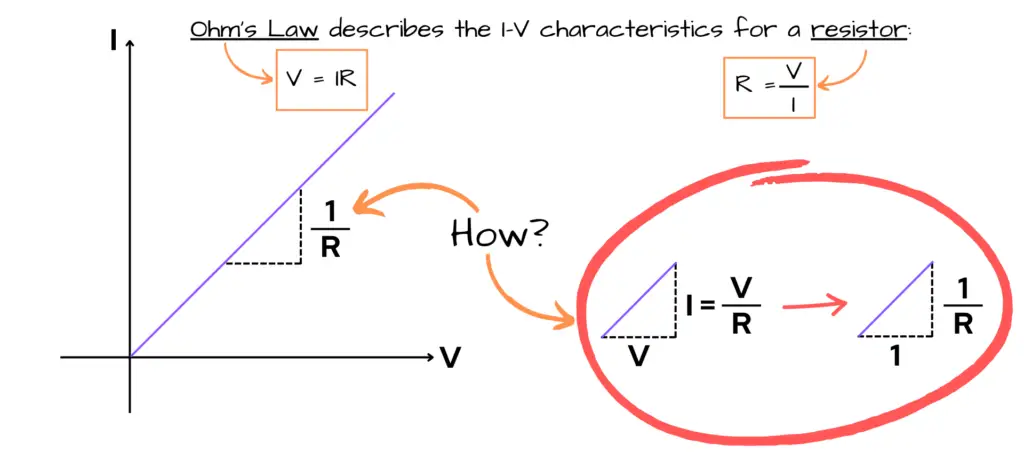
Linear/Ohmic Region
In the linear region or ohmic region, a MOSFET experiences an increase in current when an increase in voltage across the drain and source occurs. This is a linear relationship between the voltage and current— when the voltage (VDS) increases, the current (ID) increases.
In the ohmic region the MOSFET acts like a linear circuit, and the MOSFET behaves as a resistor.
- What’s the value of that resistor?
- The value of the resistor will equal to the slope of the line. Recall Ohm’s Law:
\begin{equation}
R = \frac{V}{i}
\end{equation}
\begin{equation}
R = \frac{V}{i} = \frac{3V}{10mA} = \boxed{300\Omega}
\end{equation}

Threshold Voltage (Vth)
The threshold voltage represents the minimum gate-source voltage (VGS) that must be applied to create a conductive channel between the source and drain terminals, enabling the flow of current through the device.
The threshold voltage is the voltage at which the MOSFET transitions from the off state (non-conducting) to the on state (conducting). Below this voltage, the MOSFET remains in the off state, and very little current flows.
For an n-channel MOSFET, a positive VGS above the threshold voltage attracts electrons to form a conductive channel between the source and drain. For a p-channel MOSFET, a negative VGS is required to attract holes for channel formation.
Threshold voltages can vary significantly between different MOSFETs, typically ranging from about 0.2V to 4V or more, depending on the specific type and application.
MOSFET Body Diode
Remember earlier when we were talking about the body diode of a MOSFET? We learned that the body diode is formed between the source and drain due to the MOSFET’s structure. Let’s talk more about that.
MOSFETs have a property that when their gate-to-source voltage is zero (VGS = 0), they still conduct current in reverse, from source-to-drain. This is because that they have what’s called a parasitic diode between the source and drain, and this is what’s called an intrinsic body diode or “body diode”.
The term body diode is used to describe this reverse current path when the gate is “off” or when no voltage is applied to the gate (when VGS = 0).
Review of the Structure of a MOSFET
- Terminals:
- Gate (G): Terminal that controls the channel.
- Drain (D): Terminal where current enters the MOSFET.
- Source (S): Terminal where current exits the MOSFET.
- Channel:
- The channel is formed between the source and drain and can be either n-type (for n-channel MOSFETs) or p-type (for p-channel MOSFETs).
- Insulation:
- The gate is insulated from the channel by a thin layer of silicon dioxide (SiO2). This insulation allows the gate to control the channel without drawing current.
Two Modes of MOSFETs
There are two modes of MOSFETs: depletion-mode MOSFETs and enhancement-mode MOSFETs. Both types of MOSFETs are used to control electrical signals, but they operate differently based on their design and the way they are biased. Here’s a detailed comparison of the two:
Depletion Mode MOSFET

- Basic Operation:
- Depletion-mode MOSFETs are normally ON, meaning that for this type of MOSFET, maximum current flows from drain-to-source when no voltage is applied between the gate and source (VGS = VG – VS = 0).
- When no difference in voltage exists between the gate and source, the drain-source channel “feels” the least resistance.
- To restrict the flow of charge carriers (electrons or holes) within the channel of the depletion-type MOSFET, a voltage must be applied to its gate.
- When a gate voltage is applied to a depletion-mode MOSFET, you are depleting the charge carries of the drain-source channel, therefore making the drain-source channel more resistant to current flow, i.e. reducing its conductivity.
- Channel Type:
- N-Channel: Conductive channel is made of n-type material, allowing electrons to flow. The source is connected to a negative voltage, and it conducts when a positive voltage is applied to the gate.
- P-Channel: Conductive channel is made of p-type material, allowing holes to flow. The source is connected to a positive voltage, and it conducts when a negative voltage is applied to the gate.
- Threshold Voltage (Vth):
- The threshold voltage is typically negative for n-channel depletion MOSFETs. This means that they need a negative threshold voltage (-Vth) less than the gate-source voltage (VGS) to turn it off. The threshold voltage is typically positive for p-channel depletion MOSFETs. This means that they need a positive threshold voltage (Vth) greater than the gate-source voltage (VGS) to turn it off.
| Cutt-Off | Saturation | Linear/Ohmic | |
| Depletion N-channel | VGS < -Vth | VGS > -Vth and VDS > VP | VGS > -Vth and VDS < VP |
| Depletion P-channel | VGS > Vth | VGS < Vth and VDS < -VP | VGS < Vth and VDS > -VP |
| VGS | Gate-to-Source Voltage |
| Vth | Threshold Voltage |
| VDS | Drain-to-Source Voltage |
| VP | Pinch-off Voltage |
- Applications:
- Used in applications where a normally-on switch is required, such as in analog circuits and certain logic designs.
- Symbol and Structure:
- The symbol for a depletion-type MOSFET typically has a straight line for the gate connection, indicating its normally-on state.
Enhancement Mode MOSFET

- Basic Operation:
- Enhancement-mode MOSFETs are normally OFF when no voltage is applied to the gate. There is no conductive channel until a sufficient voltage is applied.
- Applying a positive voltage to the gate (for n-channel) creates an electric field that attracts charge carriers, forming a conductive channel.
- Channel Type:
- N-Channel: No channel exists initially; electrons are attracted to form the channel when a positive voltage is applied to the gate.
- P-Channel: Similar behavior but involves attracting holes with a negative gate voltage.
- Threshold Voltage (Vth):
- The threshold voltage for n-channel enhancement MOSFETs is typically positive (+Vth), meaning a positive gate voltage is needed to turn it on. For p-channel, the threshold voltage is negative (-Vth).
| Cut-Off | Saturation | Linear/Ohmic | |
| Enhancement N-channel | VGS < Vth | VGS > Vth and VDS > VP | VGS > Vth and VDS < VP |
| Enhancement P-channel | VGS > -Vth | VGS < -Vth and VDS < -VP | VGS < -Vth and VDS > -VP |
| VGS | Gate-to-Source Voltage |
| Vth | Threshold Voltage |
| VDS | Drain-to-Source Voltage |
| VP | Pinch-off Voltage |
- Applications:
- Widely used in digital circuits, power applications, and switching circuits due to their high efficiency and rapid switching capabilities.
- Symbols and Structure:
- The symbol for an enhancement-type MOSFET shows a dashed line for the gate connection, indicating that a voltage is necessary to enhance the channel. Don’t trust schematic symbols seen in the wild, though. Lots of people use depletion mode MOSFET symbols for enhancement mode ones, because they’re easier to draw. When in doubt, refer to the manufacturer’s datasheet. Always!

What Does Pinch-off Voltage Mean?
Pinch-off voltage refers to the specific gate-source voltage (VGS) at which the channel becomes “pinched off,” meaning the conductive channel is constricted to the point that it can no longer support an increase in drain current (ID) with further increases in the drain-source voltage (VDS).
- Definition: The pinch-off voltage (VP) is the minimum gate-source voltage (VGS) required to create a conducting channel that can support current flow, beyond which the MOSFET operates in saturation mode.
- Operation Region: Below the pinch-off voltage, the MOSFET operates in the triode region (linear region), where it can act like a variable resistor. Once VGS exceeds VP and VDS reaches the pinch-off condition, the MOSFET enters the saturation region, where it maintains a constant current regardless of increases in VDS.
- Importance: Understanding the pinch-off voltage is essential for designing circuits that utilize MOSFETs, as it influences the switching characteristics and operational efficiency of the device.
Now that we’ve gone over some key information of the MOSFET, have gathered an understanding of how MOSFETs work, and have gone over some of its types and applications, let’s look at one application in particular, as an example, to further understand how to use a MOSFET in a circuit.
Problem Solving: Using a MOSFET as a Switch
MOSFETs can be used in circuits that perform a number of applications. Let’s look at one of the simplest applications a MOSFET could be used for, and that is as a switch:
Switch Application:
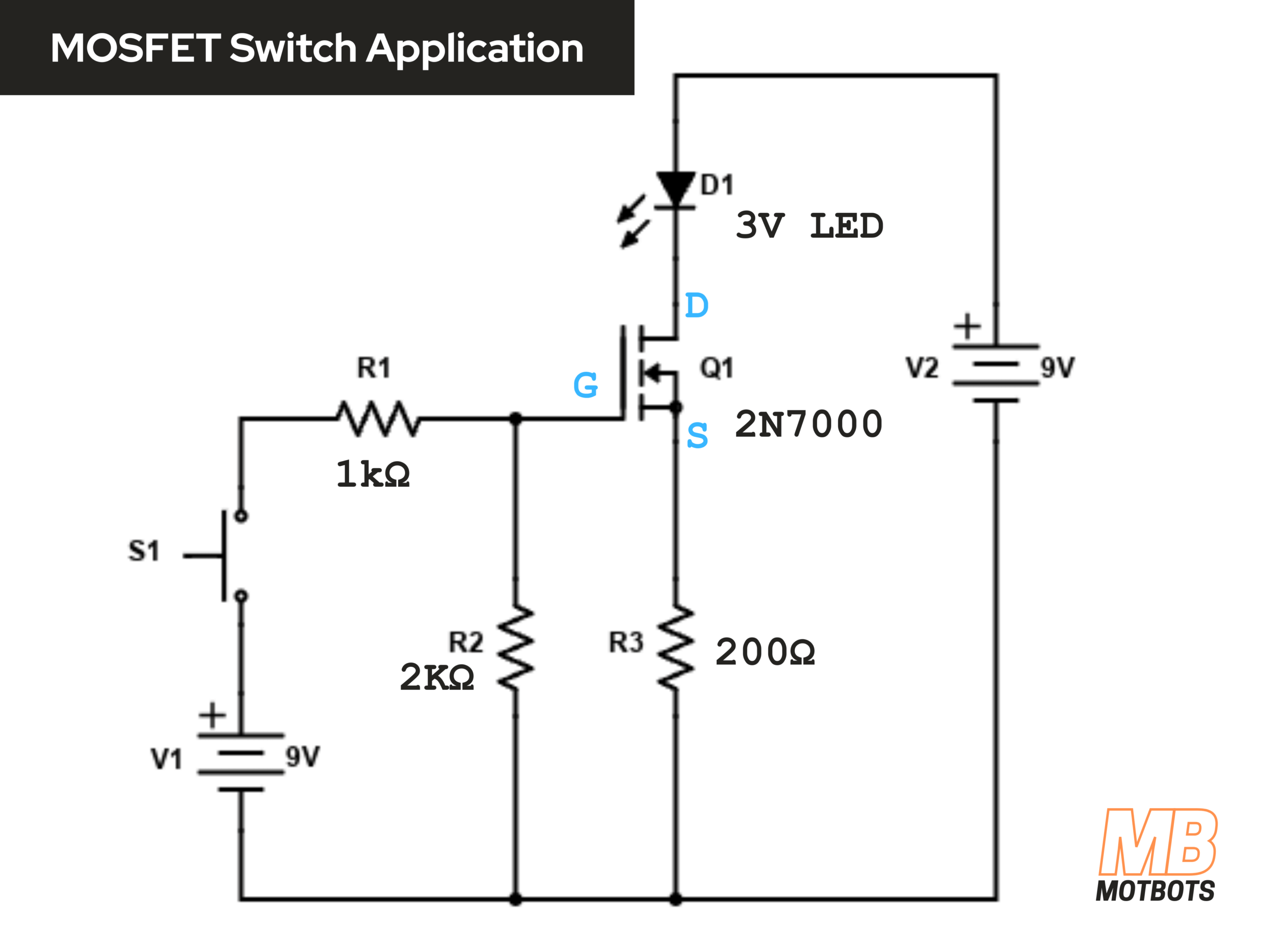
Example Circuit: Let’s say we’re given a circuit that uses a MOSFET as a switch to turn on and off an LED, and the circuit works perfectly. It uses an n-channel, enhancement mode, MOSFET for this application, as shown in the schematic below:

MOSFET Details:
- For this example, the circuit uses a 2N7000 Enhancement-mode N-channel MOSFET.
- The 2N7000 is an enhancement-mode (normally-off) transistor.
- The 2N7000 comes in a TO-92 package, which is a smaller form factor, as shown in the image below.

2N7000 N-Channel Enhancement Mode
Click to Download 2N7000 N-Channel Enhancement Mode MOSFET Datasheet
LED Details:
- For this example circuit, a 5mm round lamp green diffused LED is used. Now, that’s a mouthful!
- The green LED’s forward voltage rating ranges from 3V to 3.2V.
- Its continuous forward current rating (IF) is 20mA.


Click to Download Green LED Datasheet
Now that we have some information on the MOSFET and LED being used in the switch circuit we’ve been given, let’s look at the schematic again with some values imposed on it:

Problem to Solve:
Let’s say that we’re given some values for our circuit, but let’s say that the value of the resistor (R2) in the circuit is unreadable; that is, let’s say that the color code markings on the resistor has somehow been completely removed that we don’t know what the color bands are of the resistor. Our task will be to find the value of resistor R2.
Another value we’d like to determine for this example is to find what the drain-to-source voltage (VDS) is, once we’ve gathered the information we need from the circuit given. Let’s say that we are given the gate-source voltage (VGS), and it is 2V, when the switch (S1) is closed.
- Solve for the value of the resistor R2.
- Solve for the drain-to-source voltage, VDS.
- We are given that VGS = 2V.
- Other given values and conditions for the circuit are listed below.
Given Circuit Values:
Let’s list the values we do know, including the one we don’t, and state the current conditions of the circuit:
- Switch (S1) is a normally-open (NO) push-button switch
- With S1 OFF, there is no gate voltage on Q1 (Thanks to R2. More on this later.)
- Q1 is the 2N7000 MOSFET
- D1 is the LED
- V1 = 9V
- V2 = 9V
- R1 = 1kΩ
- R2 = ? 🤷🏻♂️
- R3 = 200Ω
R2 is Unknown:
We’re given the values for all the components used in the circuit, but one. The value of R2 is what we want to figure out for the pull-down resistance.
The pull-down resistor (R2) is important for our circuit, because its job is to make sure that when switch (S1) is off, that any charge built up on the gate (G) of Q1 may have a path to the negative supply (ground) to discharge, therefore making absolutely sure that Q1 is turned off, which is what you would want.
Now, let’s look at the schematic again when switch (S1) is pressed or in the closed position – i.e. when the switch in ON:

Conditions When Switch (S1) is Closed:
We can see that when the switch (S1) is closed, that we have a current (I) going from the positive terminal of the 9V battery (V1), through the switch. This is conventional current flow (area of positive charge to area of negative charge). Let’s make some other observations:
- Current (I): The portion of the circuit that forms a loop (loop 1) that contains V1, S1, R1, and R2 are in a series circuit. The current that flows through the resistor R2, is the current I.
- Voltage Across R2 (VR2): With current I, going through resistor R2, there’s a voltage potential that develops across R2, that we’ll call VR2.
Referring to the previous image of our circuit with the switch (S1) on, if we now turn our attention to loop 2 in the circuit that contains V2, D1, Q1, and R3, we may make some other observations:
- 9V Battery Voltage (V2): We know the value of the 9V battery (V2).
- Drain Current (ID) and Forward Voltage of LED: As per the LED’s datasheet, we’re going to use the forward current rating (IF) of 20mA as our drain current (ID) value, and a forward voltage rating of 3V for the voltage drop across the green LED in our circuit, when the switch is on. So, after we close the switch we want a drain current of 20mA, and that’s what we’ll use in our calculations.
- Drain-to-Source Voltage (VDS) and Voltage Across R3 (VR3): We must also consider the drain-to-source voltage (VDS), as well as the voltage drop across the resistor R3 (VR3) within this part of the circuit, when the switch is on.
- Source Current (IS): Since the portion of the circuit that forms the loop (loop 2) containing V2, D1, Q1, and R3, is also a series circuit, then the current leaving the source terminal (IS) of Q1 is the same current value entering the drain terminal (ID) of Q1:
\begin{equation}
\boxed{I_S = I_D = 20mA}
\end{equation}
Finding the Voltage Across R3:
Referring back to the voltage across R3 (VR3) when the circuit is activated by pressing down on the push-button switch (S1), we can calculate what that voltage is by using Ohm’s Law:
\begin{equation}
V = IR
\end{equation}
\begin{equation}
V_{R3} = I_SR_3
\end{equation}
\begin{equation}
V_{R3} = (20mA)(200Ω)
\end{equation}
\begin{equation}
V_{R3} = (0.020A)(200Ω) = 4V
\end{equation}
\begin{equation}
\boxed{V_{R3} = 4V}
\end{equation}
After finding the voltage across resistor R3 (VR3), we can update the value for it and represent this value in our schematic below:

Voltage Across R2:
We solved for the voltage across R3 (VR3), and found it to be 4V. That means that in order to have 4V across R3, the voltage across R2 (VR2) must be 6V, because the sum of the voltages for VGS and VR3 are 2V + 4V = 6V, respectively, and this voltage is in parallel with resistor R2. Recall that voltage potentials are the same for every branch parallel to each other in a circuit.

Resistor R2, will be the resistor that supplies the gate voltage. Remember, R2 is the resistor value we are trying to determine.
\begin{equation}
\boxed{V_{R2} = 6V}
\end{equation}
If the voltage across R2 is 6V, then we must have 3V across resistor R1:
\begin{equation}
\boxed{V_{R1} = 3V}
\end{equation}

Using Kirchhoff’s Voltage Law (KVL) in loop 1, starting at V1 and going around in a clockwise fashion, we can see that these voltage values must be correct:
\begin{equation}
V1 + V_{R1} + V_{R2} = 0
\end{equation}
\begin{equation}
-9V + 3V + 6V = 0
\end{equation}
\begin{equation}
\boxed{0 = 0}
\end{equation}

Current (I) Through R1 and R2:
To find the current I, that goes through resistor R1, we must recall Ohm’s Law:
\begin{equation}
V = IR
\end{equation}
\begin{equation}
V_{R1} = IR1
\end{equation}
\begin{equation}
I = \frac{V_{R1}}{R1}
\end{equation}
\begin{equation}
I = \frac{3V}{1000Ω}
\end{equation}
\begin{equation}
\boxed{I = 3mA}
\end{equation}
Knowing that loop 1 is a series circuit, we can determine that if the current I, travels through R1, then it must also travel through R2. This means that the current through R2 is also 3mA.

Solving for R2:
Since R2 is in series with R1, then the current that goes through R2 (IR2) is the same current value that goes through R1 (IR1), and that is just the current I:
\begin{equation}
\boxed{I_{R1} = I_{R2} = I = 3mA}
\end{equation}
With this information, we can now determine what the value of the resistor R2 is using Ohm’s Law:
\begin{equation}
V = IR
\end{equation}
\begin{equation}
V_{R2} = IR2
\end{equation}
\begin{equation}
R2 = \frac{V_{R2}}{I}
\end{equation}
\begin{equation}
R2 = \frac{6V}{3mA}
\end{equation}
\begin{equation}
R2 = \frac{6V}{0.003A}
\end{equation}
\begin{equation}
\boxed{R2 = 2000Ω = 2kΩ}
\end{equation}
We did it! We found the missing value of R2! At the start, we said that the circuit we were given worked ideally, and for it to do that, it’s pull-down resistor (R2) needed to be 2kΩ to do its job of discharging the gate voltage when the switch (S1) is not pressed or is open, and to provide the 4V across R3 when the switch is pressed or closed.
Using KVL to Solve for the Drain-to-Source Voltage:
If we recall Kirchhoff’s Voltage Law (KVL), we know that the loop (loop 2) containing V2, D1, Q1, and R3, must have voltage drops throughout the loop that sum to zero (0V).
If we sum the voltage values starting from the negative supply of the 9V battery (V2), going in a counter-clockwise fashion toward the forward voltage rating of 3V for the voltage drop across the LED (D1), to the drain-to-source voltage (VDS) across Q1, to the 4V across the resistor (R3) we calculated earlier, back to the negative supply of V2, we should obtain a value equal to zero:
\begin{equation}
V2 + V_{D1} + V_{DS} + V_{R3} = 0
\end{equation}
\begin{equation}
-9V + 3V + V_{DS} + 4V = 0
\end{equation}
\begin{equation}
V_{DS} = 9V – 3V -4V
\end{equation}
\begin{equation}
\boxed{V_{DS} = 2V}
\end{equation}
Checking our calculation for sanity reasons, we get:
\begin{equation}
V2 + V_{D1} + V_{DS} + V_{R3} = 0
\end{equation}
\begin{equation}
-9V + 3V + 2V + 4V = 0
\end{equation}
\begin{equation}
-9V + 9V = 0
\end{equation}
\begin{equation}
\boxed{0 = 0}
\end{equation}
We’ve just been able to figure out that the drain-to-source voltage (VDS) is equal to 2V. Sweet!

Parts List for MOSFET Switch Application
Schematic for MOSFET Switch Application
Video: Understanding MOSFETs: MOSFET as a Switch

Conclusion
We’ve introduced the MOSFET, and have even compared them to the bipolar junction transistor (BJT). We’ve briefly gone over their symbols, their structure, the different types that there are, and have even discussed how they work.
It was a lot of information to review, I know, but there’s a lot more available information out there! What was gone over here should be enough to calm your nerves, at least enough to give you a bit more confidence on your knowledge of them before you started here.
Just know that MOSFETs are vital components in modern electronics due to their ability to function as efficient switches and amplifiers. Their unique structure allows them to operate with high speed and low power consumption, making them suitable for a wide range of applications, from consumer electronics to industrial power systems. Understanding MOSFETs is essential for anyone looking to work in electronics, engineering, or related fields.
We hope that the information shared here has been beneficial to you. We appreciate you stopping by, and remember to keep at it and stay motivated!
